My Geo Map

Sponsor Links

AmericasBest.com

22 January 2009

Simple servo controller Schematic

This cicuit allows you to test a servo. The angle of the servo can be set by means of the 10k potmeter. Perhaps you will not be able to reach all positions with this circuit. Playing with other resistors may help.


Part component;

1 555 timer IC
1 BC547 transistor
1 10k Ohm potentiometer
2 10k Ohm resistors
2 100nF condensators
1 220k Ohm resistor
1 15k Ohm resistor

Telephone Audio Interface Schematic

Audio from a telephone line can be obtained using a transformer and capacitor to isolate the line from external equipment. A non-polarized capacitor is placed in series with the transformer line connection to prevent DC current from flowing in the transformer winding which may prevent the line from returning to the on-hook state. The capacitor should have a voltage rating above the peak ring voltage of 90 volts plus the on-hook voltage of 48 volts, or 138 volts total. This was measured locally and may vary with location, a 400 volt or more rating is recommended. Audio level from the transformer is about 100 mV which can be connected to a high impedance amplifier or tape recorder input. The 3 transistor amplifier shown above can also be used. For overvoltage protection, two diodes are connected across the transformer secondary to limit the audio signal to 700 mV peak during the ringing signal. The diodes can be most any silicon type (1N400X / 1N4148 / 1N914 or other). The 620 ohm resistor serves to reduce loading of the line if the output is connected to very low impedance.


Synthesized WBFM Transmitter

This project is a complete crystal-controlled Wide Band Frequency Modulated (WBFM) transmitter delivering a power output in the order of 10 mW (+10dBm) using simple components. The transmitter is based upon the Phase-Locked Loop (PLL) principle, but due to the circuit's simplicity a true "phase lock" can never be achieved.

The transmitter has both 1v peak-to-peak 'LINE' input and 10mV 'MIC' audio inputs. These will accept audio input sources from external equipment, such as hi-fi, CD and computer equipment. The microphone input also has an in-built power source to energize an 'Electret' type condenser microphone. The Radio Frequency (RF) output circuitry includes a three-pole filter for reduction of harmonics and other spurious signals. The spurious output signal level is better than -40dBc (0.0001 times the power of the wanted signal level), which makes the project suitable for driving an external power amplifier.

The transmitter is powered from a 12v supply, but it will operate from 9 Volts to 16 Volts. The DC power input is equipped with a diode (D1), which protects the transmitter in the event the supply voltage is inadvertently connected the wrong way round.

This figure is schematic the transmitter;

Construction should begin with the wire link WLK, all horizontally mounted resistors, then the power diode D1. WLK is formed from one of the resistor lead off-cuts. All vertically mounted resistors and ceramic capacitors are next, followed by the electrolytic capacitors and the four transistors. Finally, fir the vericap diode, D2, and the integrated circuits.

Although internally protected, the ICs should be fitted on a static protected workbench. In the absence of a suitable workbench, then aluminum foil can be taped to a work board and connected to the soldering iron Earth (Ground) via a 1M0 resistor. The ICs should be left in the packaging supplied until required. Before handling them, the worker should also be electrically connected to the workbench anti-static mat (foil) via a 1M0 resistor.

Note that C25 and C29 must be miniature capacitor types, due to space restrictions on the PCB. These two components should ideally be fitted after all the resistors and other components have been fitted, and the component bodies positioned about 3mm away from the PCB. These two capacitors should be mounted vertically, as shown to the right. Long component leads will have no effect on the operation of the project. The distance between TR2 / TR3 body and the PCB must be at least 4mm minimum and no greater than 6mm. 4mm is required for clearance between TR3 and L3.

Failure to observe this may cause the collector of TR3 to touch L3 causing a collector-emitter short circuit. A good tip is to fit TR2 and TR3 after L3 has been fitted. L3 should be fitted touching the PCB. C30 has been added to the circuit to restrict the upper operating frequency of the transmitter. 4p7 restricts this to approximately 125MHz. Without C30 fitted the transmitter is capable of operation over 150MHz. It is possible that certain manufacturers of IC1 produce a slightly less sensitive version. If this is used then C7 may be increased in value to 120pf.

Simple Circuit - Detects Voltage Over Ranges

Sometimes, a visual indication of whether a sensed voltage is above or below its nominal value can be useful. Most approaches to over voltage or under voltage sensing use two voltage comparators and a resistor divider to form a window comparator. The circuit in Figure 1a is an alternative to the traditional window-comparator approach. It provides different-color indications if the sensed voltage is above or below the preset value; in this case, it is centered around 0V.


The circuit uses a FET-input, low-offset-voltage OPA124 op amp and a dual-color LED. The forward voltages for the red and green LED sections are 2 and 2.1V, respectively. The values of the op-amp feedback resistors R1 and R2 are such that the op amp's closed-loop gain, 1+R2/R1, equals VLED/VWIN, where VWIN is the desired positive or negative window threshold. Thus, whenever the input voltage, VIN, exceeds ±VWIN in magnitude, the op-amp stage supplies a voltage that turns on the corresponding LED. When VIN>+VWIN, the red LED turns on; when VIN<–VWIN, the green LED turns on. Whenever –VWIN<+VWIN, both the red and green LEDs are off. R3, typically 5 kV, limits the maximum on-state LED current. You should choose R1 such that the feedback current through R3 is small compared with the on-state LED current. You can ignore the small difference between the red and green LED forward voltages for most applications, or you can balance it by adjusting the op-amp offset voltage. For asymmetrical window voltages, you can use the configuration in Figure 1b. In this case, you assume |VWIN–|>|VWIN+|, where |VWIN–| is the magnitude of the negative window voltage and |VWIN+| is the magnitude of the positive window voltage. Q1 is an NMOS enhancement-mode MOSFET that has a threshold voltage of approximately 1V. The source terminal of Q1 connects to the negative input of the op amp; thus, it remains at a virtual-ground potential. The gate terminal connects to the op amp's output, which turns Q1 on whenever the output voltage exceeds Q1's threshold voltage.

For input voltages greater than 0V, the op amp produces a negative voltage and Q1 turns off. The ratio of R2 and R1 sets the op-amp gain, and the output clamps at the on-state voltage of the green LED, approximately –2.1V. For input voltages lower than 0V, Q1 turns on once the op amp's output exceeds the threshold voltage of Q1. In this case, the ratio of R1 and the parallel combination of R2 and R3 sets the op-amp gain, and the maximum output voltage is the on-state voltage of the red LED, 2V. Resistor R4 again serves as a current limiter for the LEDs. The relationship between the resistor values and the positive and negative window voltages is given by the following equations. For simplicity, we use only the positive magnitude of the voltages, and we neglect the difference between the forward voltages of the red and green LEDs.


You should choose the value of R1 such that the feedback current through R4 is small in comparison with the on-state LED current. Choose R3 such that its value is much greater than the on-resistance of Q1. The op-amp configuration in Figure 2 has resistor values that set the VWIN– window at –5V and the VWIN+ window at 0.8V. For the case in which |VWIN–|<|VWIN+|, you can replace Q1 with an equivalent PMOS enhancement-mode MOSFET. When the window voltages VWIN– and VWIN+ have the same polarity, you can also use the circuit in Figure 2.

This circuit inserts a unity-gain difference amplifier (for example, an INA105) in the front end of the circuit in Figure 1a. This added stage subtracts a reference voltage, VR. You can use this type of window-comparator circuit to monitor a power-supply voltage, such as 5V, with preset limits of 4.75 and 5.25V, for example. The following equations yield the window voltages: Source: Mark Stitt, Burr-Brown, Tucson, AZ

QRP HF LINEAR AMPLIFIER Schematic

This project was a particular surprise for me in that the BC547 (equiv 2N2222) can be used to build a 500mW linear amplifier covering the entire HF band with excellent spectral purity and no neutralizing at all. Ugly-bug construction was used but I dare say that the good results are partly to do with the method of construction.

The circuit is fairly straight-forward and does not even need any form of RF neutralizing. Two pairs of BC547 transistors are used in a push-pull type of output stage, biased by a single diode and resistor. The driver is also very conventional using T1 to transform the drive impedance to a very low value for the output pairs. The amplifier is constructed on a piece of copper-clad board 45mm long by 17mm wide. Superglue a 44mm long by 3mm wide strip of copper-clad board along the center. This will become the battery supply rail. Using a sharp knife, remove some copper to form a 3mm x 3mm pad at one end of the battery rail to form the RF output terminal. Next fit the 10n and 33n is decoupling capacitors; one pair at either end. These should lay flat on the board. The rest is easy after you see the photographs.

T1 primary is 14-turns of very thin wire (0.1mm Dia.) and the secondary is 1+1 turn of thin wire (0.2mm Dia.). T1 former is two of the smallest ferrite beads I could find. You can just see it in the left-hand photograph above. T1 is composed of two grey ferrite beads. The right-hand photograph shows T2 and the mounting of the two output pairs of BC547 transistors.

T2 is a little special. I found two small ferrite rings in the junk-box and decided to give them a try. The windings are 11-turns three flar wound using thin wire (0.2mm Dia.):

· Twist together three 1-metre lengths of thin enameled wire.
· Wind 11-turns through the ferrite rings (1-turn is passed through both rings). Do NOT cut off the surplus yet.
· Identify A1-A2, B1-B2, C1-C2 using an ohm-meter.
· Thread each end of C1 and C2 back through the ferrite rings to add 2-1/2 extra turns to each end. Winding C should now have a total of 16-turns.
· Twist together A2 and B1 and connect to the positive battery rail.
· Connect A1 and B2 to the BC547 collectors.

The five transistors are all mounted on their heads using super-glue and with their legs in the air spread wide apart. The finished linear amplifier does not look very pretty but it is very small. It is less than 10mm high and looks like this. Here you can see it beside my parker pen for comparison (I thought it would be better than a common 1-crown coin).

Power Supply Theory

Power supply is a reference to a source of electrical power. A device or system that supplies electrical or other types of energy to an output load or group of loads is called a power supply unit or PSU. The term is most commonly applied to electrical energy supplies, less often to mechanical ones, and rarely to others.

This term covers the power distribution system together with any other primary or secondary sources of energy such as:
· Conversion of one form of electrical power to another desired form and voltage. This typically involves converting 120 or 240 volt AC supplied by a utility company (see electricity generation) to a well-regulated lower voltage DC for electronic devices. For examples, see switched-mode power supply, linear regulator, rectifier and inverter (electrical).
· Batteries
· Chemical fuel cells and other forms of energy storage systems
· Solar power
· Generators or alternators (particularly useful in vehicles of all shapes and sizes, where the engine has torque to spare, or in semi-portable units containing an internal combustion engine and a generator) (For large-scale power supplies, see electricity generation.) Low voltage, low power DC power supply units are commonly integrated with the devices they supply, such as computers and household electronics.

Constraints that commonly affect power supplies are the amount of power they can supply, how long they can supply it without needing some kind of refueling or recharging, how stable their output voltage or current is under varying load conditions, and whether they provide continuous power or pulses.

The regulation of power supplies is done by incorporating circuitry to tightly control the output voltage and/or current of the power supply to a specific value. The specific value is closely maintained despite variations in the load presented to the power supply's output, or any reasonable voltage variation at the power supply's input. This kind of regulation is commonly categorized as a Stabilized power supply.

Power supply types
Power supplies for electronic devices can be broadly divided into linear and switching power supplies. The linear supply is a relatively simple design that becomes increasingly bulky and heavy for high current devices; voltage regulation in a linear supply can result in low efficiency. A switched-mode supply of the same rating as a linear supply will be smaller, is usually more efficient, but will be more complex.

Linear power supply
An AC powered linear power supply usually uses a transformer to convert the voltage from the wall outlet (mains) to a different, usually a lower voltage. If it is used to produce DC, a rectifier is used. A capacitor is used to smooth the pulsating current from the rectifier. Some small periodic deviations from smooth direct current will remain, which is known as ripple. These pulsations occur at a frequency related to the AC power frequency (for example, a multiple of 50 or 60 Hz).
The voltage produced by an unregulated power supply will vary depending on the load and on variations in the AC supply voltage. For critical electronics applications a linear regulator will be used to stabilize and adjust the voltage. This regulator will also greatly reduce the ripple and noise in the output DC current. Linear regulators often provide current limiting, protecting the power supply and attached circuit from over current.

Adjustable linear power supplies are common laboratory and service shop test equipment, allowing the output voltage to be set over a wide range. For example, a bench power supply used by circuit designers may be adjustable up to 30 volts and up to 5 amperes output. Some can be driven by an external signal, for example, for applications requiring a pulsed output.
The simplest DC power supply circuit consists of a single diode and resistor in series with the AC supply. This circuit is common in rechargeable flashlights.

AC/ DC supply
In the past mains electricity was supplied as DC in some regions, AC in others. Simple, cheap, linear power supply is running directly from either AC or DC mains, often without a transformer used. They used a rectifier and capacitor filter; the rectifier was essentially a conductor, having no sudden effect when operating from DC.

Switched-mode power supply
A switched-mode power supply (SMPS) works on a different principle. AC mains input is directly rectified without the use of a transformer, to obtain a DC voltage. This voltage is then sliced into small pieces by a high-speed electronic switch. The size of these slices grows larger as power output requirements increase.

The input power slicing occurs at a very high speed (typically 10 kHz — 1 MHz). High frequency and high voltages in this first stage permit much smaller step down transformers than are in a linear power supply. After the transformer secondary, the AC is again rectified to DC. To keep output voltage constant, the power supply is need a sophisticated feedback controller to monitor current draw by the load.

Modern switched-mode power supplies often include additional safety features such as the crowbar circuit to help protect the device and the user from harm.[1] In the event that an abnormal high current power draw is detected, the switched-mode supply can assume this is a direct short and will shut itself down before damage is done. For decades PC computer power supplies have also provided a power good signal to the motherboard which prevents operation when abnormal supply voltages are present.

Switched mode power supplies have an absolute limit on their minimum current output. They are only able to output above certain wattage and cannot function below that point. In a no-load condition the frequency of the power slicing circuit increases to great speed, causing the isolation transformer to act as a Tesla coil, causing damage due to the resulting very high voltage power spikes. Switched-mode supplies with protection circuits may briefly turn on but then shut down when no load has been detected. A very small low-wattage dummy load such as a ceramic power resistor or 10 watt light bulb can be attached to the supply to allow it to run with no primary load attached.

Power factor has become a recent issue of concern for computer manufacturers. Switched mode power supplies have traditionally been a source of power line harmonics and have a very poor power factor. Many computer power supplies built in the last few years now include power factor correction built right into the switched-mode supply, and may advertise the fact that they offer 1.0 power factor.

By slicing up the sinusoidal AC wave into very small discrete pieces, the portion of the AC current not used stays in the power line as very small spikes of power that cannot be utilized by AC motors and results in waste heating of power line transformers. Hundreds of switched mode power supplies in a building can result in poor power quality for other customers surrounding that building, and high electric bills for the company if they are billed according to their power factor in addition to the kilowatts used. Filtering capacitor banks may be needed on the building power mains to suppress and absorb these negative power factor effects.

Low Power LED Battery Voltmeter Schematic


This is a low power voltmeter circuit that can be used with alternative energy systems that run on 12 and 24 volt batteries. The voltmeter is an expanded scale type that indicates small voltage steps over the 10 to 16 volt range for 12 volt batteries and over the 22 to 32 volt range for 24 volt batteries. Power consumption can be as low as 14mw when operated from 12V and 160mw when operated from 24V. It is possible to set the meter to read equal steps across a variety of upper and lower voltages. The meter saves power by operating in a low duty-cycle blinking mode where the LED indicators are only on and consuming power briefly during a repeating 2 second cycle. The circuit may be switched to a high power mode where the active LED stays on at all times.

Different colored LEDs may be used for the voltage level indicator, this allows the battery state to be read in the dark. With the new blue LEDs, it is possible to have a nice looking rainbow of colors using two each of red, amber, yellow, green, and blue LEDs. The circuit will also work with inexpensive and common red LEDs. If the circuit is to be used in sunlight, ultra-bright LEDs should be used, although even those may be hard to read without some kind of sun shield. The circuit may be built with either the CMOS ICM7555 timer or the more common bipolar 555 timer. The 7555 timer will provide much more efficient operation and should be used for systems with small batteries.

Theory for 12 Volt operation
The heart of the circuit is the LM3914N dot-bar volt meter IC, U2. This chip is operated in the expanded-scale mode so that the circuit responds in the 10-16V range. U2 outputs a steady voltage on pin 7 from the internal voltage reference. This is fed via voltage dividers VR2 and R5 to the internal reference input pins to set the range that the meter is sensitive to. The measured voltage is fed in on pin 5 via the voltage divider consisting of R4 and VR1. This divider scales the input voltage down to a range that is useful to the IC.

The U2 positive supply is connected to pin 3 which is nominally 12V. The U2 negative supply is switched on momentarily via transistor Q1, this switching action is what makes the circuit efficient since U1 (ICM7555) consumes a mere 0.34 ma while U2 consumes around 18ma with one LED on. The ICM7555 timer, U1 is wired to run in a free-running mode with a narrow pulse width square wave output.

The duty-cycle of U1 is controlled by the ratio of R1 and R2. R2 may be adjusted to a smaller value if faster blinking is desire, a potentiometer may be substituted for R2 if a rate adjustment is desired. R1 may be increased if a longer on-time is desired. Changes in R1 and R2 will affect the average current that the circuit consumes. The frequency of oscillation is determined by C1, R1, and R2. C1 may be either an electrolytic or poly capacitor, if an electrolytic part is used, be sure to connect the positive terminal to U1 pins 6 and 2 and the negative terminal to ground.

The output of the timer IC is fed through current limiting resistor R3 to transistor Q1 which controls power to U2. Capacitor C2 filters the control voltage input to U1 and capacitor C3 provides DC filtering for the whole circuit. When the lock-on switch across capacitor C1 is closed, the output of the timer remains on, thus enabling the U2 circuitry and increasing the current drain to 18mA. The reason the switch is not simply wired across the transistor is to keep the negative supply to U2 the same as when the circuit is pulsed on. This maintains the same calibration on the LEDs in both modes because the transistor's voltage drop is always part of the circuit.

Last, but not least, fuse F1 protects against the potential for fire hazard should the circuit become shorted out. The average current is calculated by adding the constant current required by U1 with the product of the current from U2 times the duty cycle, see the specifications for details. To operate the circuit in the 12V mode, wire the circuit so that jumpers J2 and J5 are shorted, parts U3, C4, R6, and R7 may be left out.

Theory for 24 Volt operation
When wired for 24 Volt operations, the meter responds in the 20-32V range. R6 is connected to the 24V supply instead of R4, the greater value of R6 scales the higher input voltage to a range that is useful for U2. Voltage regulator U3 with series resistor R7 scales the 24V down to a regulated 12V to provide the proper operating voltage for the ICs. Resistor R7 assures that the input voltage to the regulator stays well below the 35V absolute maximum specification of the IC. Operation in 24V mode is less efficient than in 12V mode because of the extra power dissipated by the voltage regulator and R7. To operate the circuit in the 24V mode, wire the circuit so that jumpers J1, J3, and J4 are shorted. R4 may be left out in the 24V mode.

LED Photo Sensor Circuit


This is a circuit that takes advantage of the photo-voltaic voltage of an ordinary LED. The LED voltage is buffered by a junction FET transistor and then applied to the inverting input of an op-amp with a gain of about 20. This produces a change of about 5 volts at the output from darkness to bright light. The 100K potentiometer can be set so that the output is around 7 volts in darkness and falls to about 2 volts in bright light.

Low Power FM Transmitter Schematic

The circuit of the transmitter is shown in Figure 1, and as you can see it is quite simple. The first stage is the oscillator, and is tuned with the variable capacitor. Select an unused frequency, and carefully adjust C3 until the background noise stops (you have to disable the FM receiver's mute circuit to hear this).

Because the trimmer cap is very sensitive, make the final frequency adjustment on the receiver. When assembling the circuit, make sure the rotor of C3 is connected to the +9V supply. This ensures that there will be minimal frequency disturbance when the screwdriver touches the adjustment shaft. You can use a small piece of non copper-clad circuit board to make a screwdriver - this will not alter the frequency.

The frequency stability is improved considerably by adding a capacitor from the base of Q1 to ground. This ensures that the transistor operates in true common base at RF. A value of 1nF (ceramic) as shown is suitable, and will also limit the HF response to 15 kHz - this is a benefit for a simple circuit like this, and even commercial FM is usually limited to a 15kHz bandwidth.

The Principle of works this application;
Q1 is the oscillator, and is a conventional design. L1 and C3 (in parallel with C2) tune the circuit to the desired frequency, and the output (from the emitter of Q1) is fed to the buffer and amplifier Q2. This isolates the antenna from the oscillator giving much better frequency stability, as well as providing considerable extra gain. L2 and C6 form a tuned collector load, and C7 helps to further isolate the circuit from the antenna, as well as preventing any possibility of short circuits should the antenna contact the grounded metal case that would normally be used for the complete transmitter.

The audio signal applied to the base of Q1 causes the frequency to change, as the transistor's collector current is modulated by the audio. This provides the frequency modulation (FM) that can be received on any standard FM band receiver. The audio input must be kept to a maximum of about 100mV, although this will vary somewhat from one unit to the next. Higher levels will cause the deviation (the maximum frequency shift) to exceed the limits in the receiver - usually ±75kHz.

With the value shown for C1, this limits the lower frequency response to about 50Hz (based only on R1, which is somewhat pessimistic) - if you need to go lower than this, then use a 1uF cap instead, which will allow a response down to at least 15Hz. C1 may be polyester or mylar, or a 1uF electrolytic may be used, either bipolar or polarise. If polarised, the positive terminal must connect to the 10k resistor.

Current Divider Theory

In electronics, a current divider is a simple linear circuit that produces an output current (IX) that is a fraction of its input current (IT). Current division refers to the splitting of current between the branches of the divider. The currents in the various branches of such a circuit will always divide in such a way as to minimize the total energy expended. This can be shown by calculus.

The formula describing a current divider is similar in form to that for the voltage divider. However, the ratio describing current division places the impedance of the unconsidered branches in the numerator, unlike voltage division where the considered impedance is in the numerator. This is because in current dividers, total energy expended is minimized, resulting in currents that go through paths of least impedance, therefore the inverse relationship with impedance. On the other hand, voltage divider is used to satisfy Kirchoff's Voltage Law. The voltage around a loop must sum up to zero, so the voltage drops must be divided evenly in a direct relationship with the impedance.

To be specific, if two or more impedances are in parallel, the current that enters the combination will be split between them in inverse proportion to their impedances (according to Ohm's law). It also follows that if the impedances have the same value the current is split equally.


Circuit Detector and Disconnecting Over Voltage Schematic

The circuit in this figure is protecting the circuit and the system with power supplies that may exceed safe limits. One example is small consumer products that use external ac adapters; it's easy to mistakenly plug in the wrong adapter. Another example is a portable system that uses a rechargeable battery pack. If the battery pack is absent or fails to open during recharging, a high-compliance charger can deliver excessive voltages to the system.


The circuit works using LM4041 adjustable shunt-voltage regulator as a voltage detector. When it operates as a reference, the LM4041 develops a voltage across its positive and negative terminals. This signal forces the voltage across R1 to equal 1.24V. In this circuit, however, R3 prevents this servo action. With R3 in the circuit, VG is near ground when the voltage across R1 is less than 1.24V, and VG is approximately 1V below the positive rail when the voltage across R1 is greater than 1.24V. You can, therefore, set a threshold voltage by selecting appropriate values of R1 and R2. When the supply voltage exceeds the threshold, VG goes high, thereby turning off Q1 and removing power from the load. Select R1 and R2 according to:

It where VSHUTOFF is the supply voltage that causes shutoff. With the values shown, the circuit removes power from the load when the supply voltage reaches approximately 6V. R4 provides hysteresis to prevent chattering when the supply voltage is near the shutoff value. IC1 can accommodate shutoff voltages as high as 10V; clamping IC1's supply voltage with another inexpensive shunt reference or zener diode (across the positive and negative terminals) allows higher maximum shutoff voltages. Maximum supply voltage with the components is approximately 50V.

AC Current Monitor Schematic

Parts:

R1,R2,R8 1K 1/4W Resistors

R3,R4 220K 1/4W Resistors

R5 100R 1/4W Resistor (See Notes)

R6 10K 1/2W Trimmer Cermet

R7,R10 1M 1/4W Resistors

R9 22K 1/2W Resistor

R11 to R17 1K 1/4W Resistors

C1,C3 100µF 25V Electrolytic Capacitors

C2,C4 1µF 63V Electrolytic Capacitors

D1 5mm. Red LED

D3,D4 1N4002 100V 1A Diodes

D2,D5,D6,D7 LEDs (Any color and size)

Q1 BC327 45V 800mA PNP Transistor

IC1 TL061 Low current BIFET Op-Amp (First version)

IC1 LM358 Low Power Dual Op-amp (Second version)

IC1 LM324 Low Power Quad Op-amp (Third version)

L1 10mH miniature Inductor (See Notes)

RL1 Relay with SPDT 2A @ 220V switch

Coil Voltage 12V. Coil resistance 200-300 Ohm

J1 Two ways output socket

This circuit was designed on request, to remotely monitor when a couple of electric heaters have been left on. Its sensor must be placed in contact with the feeder to be able to monitor when the power cable is drawing current, thus causing the circuit to switch-on a LED. The circuit and its sensor coil can be placed very far from the actual load, provided an easy access to the power cable is available.

Any type of high-current load or group of loads can be monitored, e.g. heaters, motors, washing machines, dish-washers, electric ovens etc., provided they dissipate a power comprised at least in the 0.5 - 1KW range. This design features three versions. The basic one illuminates a LED when the load is on. The second version activates a Relay when a pre-set current value flows into the power cable. The third version switches-on D7 when the load power is about 1KW, D6 when the load power is about 2KW and D5 when the load power is about 3KW.

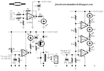
The basic circuit is shown top left in the drawing and must be used in all three versions. IC1 acts as a differential amplifier having a gain of 220. The small AC voltage picked-up by L1 is therefore amplified to a value capable of driving the LED D1.

The second version is drawn bottom left, must be connected to the basic circuit and uses a dual op-amp: therefore IC1 will be labeled IC1A and its pin layout varies slightly. IC1B acts as a voltage comparator and its threshold voltage can be precisely set by means of trimmer R6. Q1 is the Relay driver and D2 illuminates when the Relay is on. You can use the Relay contacts to drive an alarm or a lamp when the AC load exceeds a pre-set value, e.g. 2KW.

The third version is shown to the right of the drawing, must be connected to the basic circuit and uses a quad op-amp, therefore IC1 will be labeled IC1A and its pin layout varies slightly. IC1B, C and D are wired as comparators. They switch on and off the LEDs, referring to voltages at their non-inverting inputs set by the voltage divider resistor chain R11-R14.

19 January 2009

Low Frequency Sine wave Generators Schematic


The two circuits below illustrate generating low frequency sine waves by shifting the phase of the signal through an RC network so that oscillation occurs where the total phase shift is 360 degrees. The transistor circuit on the right produces a reasonable sine wave at the collector of the 3904 which is buffered by the JFET to yield a low impedance output. The circuit gain is critical for low distortion and you may need to adjust the 500 ohm resistor to achieve a stable waveform with minimum distortion. The transistor circuit is not recommended for practical applications due to the critical adjustments needed.


The op-amp based phase shift oscillator is much more stable than the single transistor version since the gain can be set higher than needed to sustain oscillation and the output is taken from the RC network which filters out most of the harmonic distortion. The sine wave output from the RC network is buffered and the amplitude restored by the second (top) op-amp which has gain of around 28dB.

Frequency is around 600 Hz for RC values shown (7.5K and 0.1uF) and can be reduced by proportionally increasing the network resistors (7.5K). The 7.5K value at pin 2 of the op-amp controls the oscillator circuit gain and is selected so that the output at pin 1 is slightly clipped at the positive and negative peaks. The sine wave output at pin 7 is about 5 volts p-p using a 12 volt supply and appears very clean on a scope since the RC network filters out most all distortion occurring at pin 1.

High Impedance FET And RF-spectrum analyzers


Current models of spectrum analyzers routinely offer frequency responses that begin as low as 10 Hz. When you combine them with 1-Hz or narrower band FFT software, expanded low-frequency performance makes the modern spectrum analyzer an invaluable tool for designing and debugging high-performance analog circuits. Unfortunately, a spectrum analyzer that’s primarily for RF typically presents an input impedance of 50, a heavy load when you apply it to most high impedance analog circuits. You can improvise a some what higher impedance probe by adding a 953 resistor in series with the 50 input, but this approach provides only 1K input impedance and reduces the measured signal by 26 dB. In addition, most RF-spectrum analyzers lack ac coupling, and, thus, any dc-input component directly reaches either the internal terminating resistor or the front-end mixer.


To maintain a 10-Hz, low-frequency response, you must connect a coupling capacitor with a value of at least 2F in series with the 953 input probes. Although oscilloscopes’ input circuits can withstand accidental probe contacts and capacitive-transient overloads, using a low impedance, ac-coupled probe with a spectrum analyzer can lead to destruction of the analyzer’s expensive and possibly hard-to-replace front-end mixer. Although high-impedance probes are commercially available, they’re expensive to purchase and repair. This Design idea offers an alternative: an inexpensive and well-protected unity-gain probe that presents the same input impedance as a basic bench oscilloscope and can drive the spectrum analyzer is 50 input impedances. The probe has a gain of 0 - 0.2 dB at 100 kHz. Input impedance is 1 M, 15 pF, and maximum input is 0.8V p-p. Load impedance is 50, and frequency response is 10 Hz to 200 MHz at 3 dB. Pass band ripple is less than 1 dB p-p.


Input noise at 1 MHz is less than 10 nV/Hz. Distortion for 0.5V p-p input at 10 MHz is less than 75 dBc for second-order distortion and less than 85 dBc for third order. Power requirements are 5V at 16 mA. You can assemble the circuit in the figure readily available and inexpensive components. The circuit’s input presents the same characteristics as a bench oscilloscope 1-M resistance in parallel with 15 pF of capacitance. You can also use this active probe in place of standard 1-to-1 or 10-to-1 oscilloscope probes, thus extending the designs applicability. The back-to-back silicon diodes in the D1 clamp the input signal to plus or minus one forward-voltage drop, which limits signal excursions you apply to the spectrum analyzer’s front end, thus protecting the input mixer from damage due to overloads and ESD.


Because most users employ the probe and spectrum analyzer to measure small-amplitude signals and noise, the limited large-signal response does not affect most applications. High-performance FET input operational amplifier IC1, a Texas Instruments OPA656, provides a voltage gain of two. This configuration yields a bandwidth of approximately 200 MHz the OPA656 can drive 50 back-matched loads for a total load of 100, which results in a 6-dB gain loss for which IC1’s gain of two compensates for a net gain of unity. The OPA656 also introduces lower noise and distortion than that of most commercially available, active FET-based probes.


The probe in the figure fits into a small section of brass hobby tubing. The input connector comprises a small SMA edge-launch connector that you can easily adapt to other connectors, including the BNC and its many accessories. The probe requires 5 and 5V at approximately 18 mA each, which you can obtain from an instruments probe-power connector if available or from a linear supply designed around an ac wall transformer. For best results, use 78L05 and 79L05 voltage regulators to stabilize the supply voltages. Standard miniature 50 coaxial cable connects the probe to the measuring instrument. For the flattest frequency response and uniform gain, terminate the probes output with 50, the circuit requires no dc-output-blocking capacitor

Low Power LED Battery Voltmeter


This is a low power voltmeter circuit that can be used with alternative energy systems that run on 12 and 24 volt batteries. The voltmeter is an expanded scale type that indicates small voltage steps over the 10 to 16 volt range for 12 volt batteries and over the 22 to 32 volt range for 24 volt batteries. Power consumption can be as low as 14mw when operated from 12V and 160mw when operated from 24V.


It is possible to set the meter to read equal steps across a variety of upper and lower voltages. The meter saves power by operating in a low duty-cycle blinking mode where the LED indicators are only on and consuming power briefly during a repeating 2 second cycle. The circuit may be switched to a high power mode where the active LED stays on at all times.

Different colored LEDs may be used for the voltage level indicators, this allows the battery state to be read in the dark. With the new blue LEDs, it is possible to have a nice looking rainbow of colors using two each of red, amber, yellow, green, and blue LEDs. The circuit will also work with inexpensive and common red LEDs. If the circuit is to be used in sunlight, ultra-bright LEDs should be used, although even those may be hard to read without some kind of sun shield.

The heart of the circuit is the LM3914N dot-bar volt meter IC, U2. This chip is operated in the expanded-scale mode so that the circuit responds in the 10-16V range.

U2 outputs a steady voltage on pin 7 from the internal voltage reference. This is fed via voltage dividers VR2 and R5 to the internal reference input pins to set the range that the meter is sensitive to. The measured voltage is fed in on pin 5 via the voltage divider consisting of R4 and VR1. This divider scales the input voltage down to a range that is useful to the IC.

The U2 positive supply is connected to pin 3 which is nominally 12V. The U2 negative supply is switched on momentarily via transistor Q1, this switching action is what makes the circuit efficient since U1 (ICM7555) consumes a mere 0.34 ma while U2 consumes around 18ma with one LED on. The ICM7555 timer, U1 is wired to run in a free-running mode with a narrow pulse width square wave output.

The duty-cycle of U1 is controlled by the ratio of R1 and R2. R2 may be adjusted to a smaller value if faster blinking is desire, a potentiometer may be substituted for R2 if a rate adjustment is desired. R1 may be increased if a longer on-time is desired. Changes in R1 and R2 will affect the average current that the circuit consumes. The frequency of oscillation is determined by C1, R1, and R2. C1 may be either an electrolytic or poly capacitor, if an electrolytic part is used, be sure to connect the positive terminal to U1 pins 6 and 2 and the negative terminal to ground.

The output of the timer IC is fed through current limiting resistor R3 to transistor Q1 which controls power to U2. Capacitor C2 filters the control voltage input to U1 and capacitor C3 provides DC filtering for the whole circuit. When the lock-on switch across capacitor C1 is closed, the output of the timer remains on, thus enabling the U2 circuitry and increasing the current drain to 18ma. The reason the switch is not simply wired across the transistor is to keep the negative supply to U2 the same as when the circuit is pulsed on. This maintains the same calibration on the LEDs in both modes because the transistor's voltage drop is always part of the circuit.

Last, but not least, fuse F1 protects against the potential for fire hazard should the circuit become shorted out. The average current is calculated by adding the constant current required by U1 with the product of the current from U2 times the duty cycle, see the specifications for details. To operate the circuit in the 12V mode, wire the circuit so that jumpers J2 and J5 are shorted, parts U3, C4, R6, and R7 may be left out.

When wired for 24 Volt operations, the meter responds in the 20-32V range. R6 is connected to the 24V supply instead of R4, the greater value of R6 scales the higher input voltage to a range that is useful for U2. Voltage regulator U3 with series resistor R7 scales the 24V down to a regulated 12V to provide the proper operating voltage for the ICs. Resistor R7 assures that the input voltage to the regulator stays well below the 35V absolute maximum specification of the IC. Operation in 24V mode is less efficient than in 12V mode because of the extra power dissipated by the voltage regulator and R7. To operate the circuit in the 24V mode, wire the circuit so that jumpers J1, J3, and J4 are shorted. R4 may be left out in the 24V mode.


Circuit add fold back-current protection schematic

For many applications that require power-supply currents of a few amperes or less, three-terminal adjustable-output linear voltage regulators, such as National Semiconductors LM317, offer ease of use, low cost, and full on-chip overload protection. The addition of a few components can provide a three-terminal regulator with high-speed short-circuit current limiting for improved reliability. The current limiter protects the regulator from damage by holding the maximum output current at a constant level, IMAX, that doesn’t damage the regulator. When a fault condition occurs, the power dissipated in the pass transistor equals approximately VIN/IMAX. Designing a regulator to survive an overload requires conservatively rated and often overdesigned components unless you can reduce, or fold back, the output current when a fault occurs.

This above figure is Figure 1


The circuit in Figure incorporates fold back current limiting to protect the pass transistor by adding feedback resistor R4. Under normal conditions, transistor Q2 doesn’t conduct, and resistors R1 and R2 bias MOSFET Q1 into conduction. When an output overload occurs, Q2 conducts, reducing the on-state bias applied to Q1 and thus increasing its drain-source resistance and limiting the current flowing into regulator IC1, an LM317. Adding R4 makes Q2’s bias current dependent on the output voltage, VOUT, which decreases under overload conditions.


For the circuit in Figure 1, you can calculate the maximum fold over and short-circuit currents, IKNEE and ISC, respectively, as follows:

In a practical design, you select values for IKNEE and ISC and equal values for R3A and R3B and then use equations 1 and 2 to calculate resistors RSC and R4. For the circuit in Figure 1, the output’s maximum and short-circuit currents are fixed at 0.7 and 0.05A, respectively. With R3A and R3B set to 100, solving the equations yields values of 0.73 for RSC and 4.3 k for R4.You can demonstrate the circuit’s performance by applying a variable-load resistor that is adjustable from 0 to 200.

As Figure 2 shows, the output is simulated and measured voltage-versus-current characteristics VOUT, respectively, are in close agreement.

Advertisement