This is the schematic diagram powers our Arduinos. For this, we can use either DC power supply or USB connection as a source. To trace how the circuit works, let us start with the 5V linear voltage regulator NCP1117ST50T3G. This regulator has a pretty straightforward function. It takes voltage input up to 20V and converts it to 5V. The Vin of this regulator is connected to the DC power supply via the M7 diode. This diode provides reverse polarity protection, which means current can only flow from the power supply to the regulator and not the other way around. This the figure of the circuit.
My Geo Map
Sponsor Links

Showing posts with label Power Supply. Show all posts
Showing posts with label Power Supply. Show all posts
08 September 2022
03 June 2020
Low Power 12V Transformerless Power Supply Circuit
Here is design
powered directly from the mains with the aid of a series capacitor (C1). The
disadvantage of this approach is that usually only one half cycle of the mains
wave-form can be used to produce a DC voltage. An obvious solution is to use a
bridge rectifier to perform full-wave rectification, which increases the amount
of current that can be supplied and allows the filter capacitor to be smaller.
The accompanying circuit in fact does this, but in a clever manner that uses
fewer components. Here we take advantage of the fact that a Zener diode is also
a normal diode that conducts current in the forward direction. During one half
wave, the current flows via D1 through the load and back via D4, while during
the other half wave it flows via D3 and D2. Bear in mind that with this circuit
(and with the bridge rectifier version), the zero voltage reference of the DC
voltage is not directly connected to the neutral line of the 230-V circuit.
This is the figure of the circuit;


10 February 2019
Car Audio Power Bridging Terms
Not only getting married is there a condition, bridging also has conditions. Because if you do not comply with these conditions then your power can be broken down in just a few hours or just a few songs with no maximum. Then what are the conditions? These conditions have been written by the manufacturer, so you should read the manual that indicates the condition if the power is in the cartridge.
Then what are the conditions? These conditions have been written by the manufacturer, so you should read the manual that indicates the condition if the power is in the cartridge. In refilling the car audio power, we should not arbitrarily connect the cable, it must be right between the pluses and minuses - that's the first condition.
30 January 2013
Over Voltage Protection Circuit
Here’s
a design circuit that called over voltage protection circuit. This circuit can
called as crowbar protection circuit. This circuit is used where we need
protection against high voltage surge. The circuit has a few components, it is
very easy to build and will protect your electric equipment again over voltages.
The crowbar circuit must be mounted between power supply and the protected
device. This is the figure of the circuit diagram;

The
over voltage protection circuit is based on brute force: when the power supply
voltage increases too much a thyristor short circuit the output. This mean that
the overvoltage is quickly removed from equipment power terminals and F1 fuse
will burn. The overvoltage (crowbar) circuit is now set. Replace the wire
bridge with a fuse (5A). In repaos state the circuit take 1 mA.
17 January 2013
Desktop PC Linear Power Supply Circuit
Here’s a
circuit for linear workbench desktop power supply
circuit converts a high input voltage (12V) from the SMPS of a PC into low
output voltage (1.25 to 9 volts). An adjustable three-pin voltage regulator
chip LM317T (IC1) is used here to provide the required voltages. The LM317T
regulator, in TO-220 pack, can handle current of up to 1 amp in practice. This
is the figure of the design circuit;

This figure shows the circuit of the desktop power supply.
Regulator IC LM317T is arranged in its standard application. Diode D1 guards
against polarity reversal and capacitor C1 is an additional buffer. The green
LED (LED1) indicates the status of the power input. Diode D2 prevents the
output voltage from rising above the input voltage when a capacitive or
inductive load is connected at the output. Similarly, capacitor C3 suppresses
any residual ripple. The circuit can be wired on a common PCB. After
fabrication, enclose the circuit in a metallic cover. Then open the cabinet of
your PC and connect the input line of the gadget to a free (hanging) four-pin
drive power connector of the SMPS carefully. Connect a standard digital
voltmeter in parallel with the output leads to accurately set the desired
voltage with the help of variable resistor VR1. You can also use your digital
multi meter if the digital voltmeter is not available. Switch on S1 and set the
required voltage through preset VR1 and read it on the digital voltmeter. Now
the power supply is ready for use.
20 August 2011
LTC3588-1 Piezoelectric Energy Harvesting Power Supply Circuit
Here’s a design circuit of The LTC3588-1 is a piezoelectric energy harvesting power supply IC that integrates a low-loss full-wave bridge rectifier with a high efficiency buck converter to form a complete energy harvesting solution optimized for high output impedance energy sources such as piezoelectric transducers. This is the figure of the circuit;

LTC3588-1 can be configured to deliver four output voltages: 1.8V, 2.5V, 3.3V and 3.6V. In this table you can see how you need to configure the pins of the LTC3588-1 to obtain the specified voltage. To select Low for D0, D1 the pin must be connected to GND and if you need to select high for D0, D2 the pin must be connected to VIN2. The maximum output current can be set up to 100mA. As you can see in this power schematic circuit the design of power supply is very easy and require few external components. A power supply circuit based on the LTC3588-1 IC offers many features like: 950nA Input Quiescent Current (Output in Regulation – No Load) , 450nA Input Quiescent Current in UVLO, 2.7V to 20V Input Operating Range, Integrated Low-Loss Full-Wave Bridge Rectifier, Up to 100mA of Output Current, Selectable Output Voltages, High Efficiency Integrated Hysteretic Buck DC/DC.
The LTC3588-1 IC can be used in many applications circuits like: Piezoelectric Energy Harvesting, Electro-Mechanical Energy Harvesting, Wireless HVAC Sensors, Mobile Asset Tracking, Tire Pressure Sensors, Battery Replacement for Industrial Sensors, Remote Light Switches.

LTC3588-1 can be configured to deliver four output voltages: 1.8V, 2.5V, 3.3V and 3.6V. In this table you can see how you need to configure the pins of the LTC3588-1 to obtain the specified voltage. To select Low for D0, D1 the pin must be connected to GND and if you need to select high for D0, D2 the pin must be connected to VIN2. The maximum output current can be set up to 100mA. As you can see in this power schematic circuit the design of power supply is very easy and require few external components. A power supply circuit based on the LTC3588-1 IC offers many features like: 950nA Input Quiescent Current (Output in Regulation – No Load) , 450nA Input Quiescent Current in UVLO, 2.7V to 20V Input Operating Range, Integrated Low-Loss Full-Wave Bridge Rectifier, Up to 100mA of Output Current, Selectable Output Voltages, High Efficiency Integrated Hysteretic Buck DC/DC.
The LTC3588-1 IC can be used in many applications circuits like: Piezoelectric Energy Harvesting, Electro-Mechanical Energy Harvesting, Wireless HVAC Sensors, Mobile Asset Tracking, Tire Pressure Sensors, Battery Replacement for Industrial Sensors, Remote Light Switches.
29 September 2010
Negative/Positive DC Voltage Power Supply Circuit
This is a design circuit for a power supply circuit that provides regulated +12V and -12V outputs. The diode bridge formed by D1, D2, D3, and D4 performs the rectification needed to convert the transformer's AC current into a DC current. By using the center tap of the transformer as ground, DC voltages of opposite polarities with respect to this ground can be generated from the transformer's AC current. This is the figure of the circuit;

During the 'positive' cycle, the transformer current travels through D1, charges up C1, goes to ground, charges up C3, travels through D3 and then returns to the opposite tap of the transformer. Note that the C1 voltage built up is positive with respect to ground while that of C3 is negative. During this cycle, D2 and D4 are 'off'.
During the 'negative' cycle, the transformer current travels through D2, charges up C1, goes to ground, charges up C3, travels through D4 and then returns to the opposite tap of the transformer. Note that this path also gives C1 and C3 a positive and a negative voltage, respectively. During this cycle, D1 and D3 are 'off'. The C1 and C3 voltages are then fed into the 7812 (+12V regulator) and 7912 (-12V regulator) IC's to come up with regulated +12V and -12V outputs, respectively.
13 March 2010
Reducing L200 Power Dissipation Circuit using Series Resistor
It’s good to reduce the power dissipated by the device. Using resistor connected in series to the input (the left figure) is a simple and economic method to reduce the device input-output differential voltage. This is the figure of the design circuit;

Here’s the formula for calculating R:
R= [Vi min- (Vo+Vdrop)]/Io
Vdrop = minimum differential voltage between the input and the output of the device at current Io
Vin min = minimum voltage
Vo = Output voltage
Io = output current
Resistor R can be connected between pins 1 and 2 of the IC instead of in series with the input if the load is constant (the right figure). So, part of the load current flows through the device and part through the resistor. This configuration is available when the minimum current by the load is:
Io min = Vdrop/R
11 February 2010
AC Power Supply Low Voltage
This is an AC power supply circuit with low voltage output (step down transformer converter). Notes! This project involves the use of dangerous voltages. You must make sure all high-voltage (120 volt household power) conductors are safely insulated from accidental contact. No bare wires should be seen anywhere on the “primary” side of the transformer circuit. Be sure to solder all wire connections so that they’re secure, and use real electrical tape (not duct tape, scotch tape, packing tape, or any other kind!) to insulate your soldered connections. If you wish to enclose the transformer inside of a box, you may use an electrical “junction” box, obtained from a hardware store or electrical supply house. If the enclosure used is metal rather than plastic, a three-prong plug should be used, with the “ground” prong (the longest one on the plug) connected directly to the metal case for maximum safety.


Before plugging the plug into a wall socket, do a safety check with an ohmmeter. With the line switch in the “on” position, measure resistance between plug prong and the transformer case. There should be infinite (maximum) resistance. If the meter registers continuity (some resistance value less than infinity), then you have a “short” between one of the power conductors and the case, which is dangerous!
Next, check the transformer windings themselves for continuity. With the line switch in the “on” position, there should be a small amount of resistance between the two plug prongs. When the switch is turned “off,” the resistance indication should increase to infinity (open circuit — no continuity). Measurement the resistance between pairs of wires is on the secondary side. These secondary windings should register much lower resistances than the primary. Why is this?
Plug the cord into a wall socket and turn the switch on. You should be able to measure AC voltage at the secondary side of the transformer, between pairs of terminals. Between two of these terminals, you should measure about 12 volts. Between either of these two terminals and the third terminal, you should measure half that. This third wire is the “center-tap” wire of the secondary winding.
25 November 2009
0 - 28V / 6 - 8A Power Supply Circuit
This is the complete design power supply circuit. This circuit has stable, clean and regulator 0-28V 6/8 Amp output voltage. This circuit is using transistor 2N3055. Although you could use this design to deliver 20 amps (with almost no modifications and with a proper transformer and a huge heat sink with a fan), it didn’t need much power. This is the figure of the circuit.

Although the 7815 power regulator will kick in on short circuit, overload and thermal overheating, the fuses in the primary section of the transformer and the fuse F2 at the output will secure your power supply. The rectified voltage of: 30 volt x SQR2 = 30 x 1.41 = 42.30 volt measured on C1. So, all the capacitors should be rated at 50 volts. Caution: 42 volt is the voltage that could be on the output if one of the transistors should blow. P1 allows you to 'regulate' the output voltage to anything between 0 and 28 volts. The LM317 lowest voltage is 1.2 volt. To have a zero voltage on the output I've put 3 diodes D7,D8 and D9 on the output of the LM317 to the base of the 2N3055 transistors. The LM317 maximum output voltage is 30 volts, but using the diodes D7,D8 & D9 the output voltage is approx 30v - (3x 0.6v) = 28.2volt. Calibrate your build-in voltmeter using P3 and, of course, a good digital voltmeter. P2 will allow you to set the limit of the maximum available amps at the output +Vcc. When using a 100 Ohm/1watt varistor the current is limited to approx. 3 Amps @ 47 Ohm and +- 1 Amp @ 100 Ohms.

Although the 7815 power regulator will kick in on short circuit, overload and thermal overheating, the fuses in the primary section of the transformer and the fuse F2 at the output will secure your power supply. The rectified voltage of: 30 volt x SQR2 = 30 x 1.41 = 42.30 volt measured on C1. So, all the capacitors should be rated at 50 volts. Caution: 42 volt is the voltage that could be on the output if one of the transistors should blow. P1 allows you to 'regulate' the output voltage to anything between 0 and 28 volts. The LM317 lowest voltage is 1.2 volt. To have a zero voltage on the output I've put 3 diodes D7,D8 and D9 on the output of the LM317 to the base of the 2N3055 transistors. The LM317 maximum output voltage is 30 volts, but using the diodes D7,D8 & D9 the output voltage is approx 30v - (3x 0.6v) = 28.2volt. Calibrate your build-in voltmeter using P3 and, of course, a good digital voltmeter. P2 will allow you to set the limit of the maximum available amps at the output +Vcc. When using a 100 Ohm/1watt varistor the current is limited to approx. 3 Amps @ 47 Ohm and +- 1 Amp @ 100 Ohms.
24 November 2009
600 Volt Power Supply
This circuit is design for power supply that can produces 600 volt. This circuit is descript a full wave voltage doubler. The output voltage is twice the input voltage. For 230V AC input the output will be nearly 600 Volts. This is the figure of the circuit.

How is the circuit work? Resister R1 is used to limit the initial high voltage and high currents. Capacitor C1, C2, C3 together with coils L1 and L2 form input line filter. The capacitors C4 and C5 protect diodes from high voltage transients on the AC line as well as reduce inter carrier hum modulation of the R.F picked up by the mains. Capacitors C6 and C7 provides enough filtering for the output DC Voltage.
Part:
C1, C2, C3 - 0.1 mf 630V
C4, C5 - 0.01 mf 630V
C6, C7 - 100 mf 450V
R1 - 10E 5W Wire Wound
R2, R3 - 220KE 2Watts
D1, D2 - BY127
D3, D4 - BY127
L1, L2 - 12 Turns 18 SWG

How is the circuit work? Resister R1 is used to limit the initial high voltage and high currents. Capacitor C1, C2, C3 together with coils L1 and L2 form input line filter. The capacitors C4 and C5 protect diodes from high voltage transients on the AC line as well as reduce inter carrier hum modulation of the R.F picked up by the mains. Capacitors C6 and C7 provides enough filtering for the output DC Voltage.
Part:
C1, C2, C3 - 0.1 mf 630V
C4, C5 - 0.01 mf 630V
C6, C7 - 100 mf 450V
R1 - 10E 5W Wire Wound
R2, R3 - 220KE 2Watts
D1, D2 - BY127
D3, D4 - BY127
L1, L2 - 12 Turns 18 SWG
12 Volt Off Line Power Supply
This is a simple circuit for switching power supply. This circuit is using converter concept. This is the figure of the circuit.

This circuit can work over an universal input AC line voltage range 90-240 VAC and provides 12 VDC output when over 4A loaded. Line and load regulation is better than 0,5%. This circuit has over current, over temperature, over voltage protection. The output ripple is approximately 0,2Volt peak to peak.
10 Amp 13, 8 Volt Power Supply
This is a design for power supply. This circuit is using LM723 for voltage regulator. This is a simple design circuit. This is the figure of the circuit.

The circuit even has a current limiting feature which is a more reliable system than most commercial units have. The circuit uses 3 pass transistors which must be heat sink. Resistor R9 allows the fine tuning of the voltage to exactly 13.8 volts and the resistor network formed by resistors R4 through R7 controls the current limiting. The LM723 limits the current when the voltage drop across R5 approaches .7 volts. To reduce costs, most commercial units rely on the HFE of the pass transistors to determine the current limiting. The fault in that system is that the HFE of the pass transistors actually increases when the transistors heat up and risks a thermal runaway condition causing a possible failure of the pass transistors. Because this circuit samples the collector current of the pass transistors, thermal runaway is not a problem in this circuit making it a much more reliable power supply.
The only adjustment required is setting R9 to the desired output voltage of anywhere between 10 and 14 volts. You may use a front panel mounted 1K potentiometer for this purpose if desired. Resistor R1 only enhances temperature stability and can be eliminated if desired by connecting pins 5 and 6 of IC-1 together. Although it really isn't needed due to the type of current limiting circuit used, over voltage protection can be added to the circuit by connecting the circuit of Figure 2 to Vout. The only way over voltage could occur is if transistors Q2 or Q3 were to fail with a collector to emitter short. Although collector to emitter shorts do happen, it is more much more likely that the transistors will open up when they fail.
20 October 2009
Transformer Voltage Booster Circuit: DC-DC Step-Up Switching Regulator Using Transistors
A DC-to-DC step-up converter is traditionally implemented using transformer, working by converting the DC voltage to AC Voltage, step-up it using transformer, then rectify and filter the transformer’s output to get a higher DC voltage. Using a switching method, we can step-up a voltage without a transformer. We just need an inductor which is driven by a switching transistor to boost the voltage. This is the figure of the circuit.

The most interesting this is that circuits use a discrete component: no integrated chip is required, only few transistors with few passive components. Because the switching topology is a boost converter, this circuit cannot be operated as step-down regulator, so the output will always be higher than the input. The voltage output is depend on the load because the feedback mechanism, through the zener diode, will maintain the output at about 14 volt, regardless the voltage input variation and load current variation. The current from the voltage divider will flow through the zener diode if the output goes higher than the nominal value, and this condition will stop the oscillator built around the 2N3904 transistors. Stopping the oscillator will drop the output voltage and thus maintain the required voltage level at the output. This transistor (Q1, Q2, and Q3) form a Schmidt trigger that drive the final transistor Q4 (the switching transistor 2N3053).
This circuit is suitable for battery booster, if you need to run your 12 volt equipments on your old car that is provide only a 6V supply from the battery. The output of this voltage double can be adjusted by changing the voltage divider, or for easier adjustment, you can replace the 4,7K resistor with a 5K potentiometer. Using a good inductor (low resistance), you can achieve up to 80% efficiency, and up to 2 Watt power can be delivered to the load. [Circuit's schematic diagram source: Bill Bowden's circuit collection]

The most interesting this is that circuits use a discrete component: no integrated chip is required, only few transistors with few passive components. Because the switching topology is a boost converter, this circuit cannot be operated as step-down regulator, so the output will always be higher than the input. The voltage output is depend on the load because the feedback mechanism, through the zener diode, will maintain the output at about 14 volt, regardless the voltage input variation and load current variation. The current from the voltage divider will flow through the zener diode if the output goes higher than the nominal value, and this condition will stop the oscillator built around the 2N3904 transistors. Stopping the oscillator will drop the output voltage and thus maintain the required voltage level at the output. This transistor (Q1, Q2, and Q3) form a Schmidt trigger that drive the final transistor Q4 (the switching transistor 2N3053).
This circuit is suitable for battery booster, if you need to run your 12 volt equipments on your old car that is provide only a 6V supply from the battery. The output of this voltage double can be adjusted by changing the voltage divider, or for easier adjustment, you can replace the 4,7K resistor with a 5K potentiometer. Using a good inductor (low resistance), you can achieve up to 80% efficiency, and up to 2 Watt power can be delivered to the load. [Circuit's schematic diagram source: Bill Bowden's circuit collection]
15 October 2009
Automatic Solar Power Supply Circuit
This circuit is almost same with 5V regulated solar power supply circuit. The different with circuit before is using diode 1N4148 and resistor that is parallel with solar panel. This is the figure of the circuit.

The oscillator will turn off when the output from the solar panel is above 1.3v and although the circuit does not shut down to zero current, it consumes about 3 mA, while the shut-off circuit takes about 1mA. On a bright day, the solar panel delivers 20mA to the battery, so the overall net charging current is about 15mA max. This means any data logging circuit or transmitter connected to the supply will only work at night.
To go over the purpose of the automatic section again: The automatic components turn off the 5v section so the battery can charge and store enough energy to operate a transmitter during the night hours, when it will be needed.

The oscillator will turn off when the output from the solar panel is above 1.3v and although the circuit does not shut down to zero current, it consumes about 3 mA, while the shut-off circuit takes about 1mA. On a bright day, the solar panel delivers 20mA to the battery, so the overall net charging current is about 15mA max. This means any data logging circuit or transmitter connected to the supply will only work at night.
To go over the purpose of the automatic section again: The automatic components turn off the 5v section so the battery can charge and store enough energy to operate a transmitter during the night hours, when it will be needed.
5V Regulated Solar Power Supply Circuit
This is a circuit of power supply that is produces a 5 VDC voltage. This circuit is rechargeable battery using solar panel. The solar panel charges the battery when sunlight is bright enough to produce a voltage above 1.9v. A diode is required between the panel and the battery as it leaks about 1mA from the battery when it is not illuminated. This is the figure of the circuit.

How is the power supply work? The regulator transistor is designed to limit the output voltage to 5v. This voltage will be maintained over the capability of the circuit, which is about 10mA. The oscillator transistor must be a high-current type as is turned on for a very short period of time to saturate the core of the transformer. This energy is then released as a high-voltage pulse. These pulses are then passed to the electrolytic and appear as a 5v supply with a capability of about 10mA. If the current is increased to 15mA, the voltage drops to about 4V. The circuit operates at approx 50 KHz and the pulses quickly charge the electrolytic.
The 15k resistor has a 3k3 "trimmer" resistor to enable you to adjust the output to exactly 5v or slightly above 5v. Microcontrollers will work up to 5.5v but some will freeze at 5.6v, so be careful. The output voltage is monitored at the join of the 15k resistor (and 3k3) and the 2k2 resistor. The voltage at this point is exactly 0.63v (630mV) and at this voltage the regulator transistor turns ON and robs the oscillator transistor with "turn-on" voltage.

How is the power supply work? The regulator transistor is designed to limit the output voltage to 5v. This voltage will be maintained over the capability of the circuit, which is about 10mA. The oscillator transistor must be a high-current type as is turned on for a very short period of time to saturate the core of the transformer. This energy is then released as a high-voltage pulse. These pulses are then passed to the electrolytic and appear as a 5v supply with a capability of about 10mA. If the current is increased to 15mA, the voltage drops to about 4V. The circuit operates at approx 50 KHz and the pulses quickly charge the electrolytic.
The 15k resistor has a 3k3 "trimmer" resistor to enable you to adjust the output to exactly 5v or slightly above 5v. Microcontrollers will work up to 5.5v but some will freeze at 5.6v, so be careful. The output voltage is monitored at the join of the 15k resistor (and 3k3) and the 2k2 resistor. The voltage at this point is exactly 0.63v (630mV) and at this voltage the regulator transistor turns ON and robs the oscillator transistor with "turn-on" voltage.
28 September 2009
Universal Power Supply Circuit
This is a design circuit for a power supply, but this design is universal power supply. This circuit is using LM371 for control operation. This is the figure of the circuit.

The Universal Power Supply output voltage can be set to anywhere in the range 1.5V to 30V by selecting two resistances. By using a potentiometer, R2, as one of the resistors you can dial up the output voltage wanted. Either AC or DC input can be supplied to the PCB via a socket or terminal block. Connection can be either way around. This is because we have provided a bridge rectifier on board. The input DC voltage to the regulator must be at least 2.5V above the required output voltage. An off/on switch is provided. The LM317 will provide slightly higher output voltages than 30 volts. To be safe for continuous operation the maximal input DC voltage to the regulator should not be over 33V. With a 2.5V to 3.0V drop across the regulator this will give a regulated output of 30V. You can draw up to 1.5A from the LM317.
When external capacitors are used with any IC regulator it is good practice to add protection diodes to prevent the capacitors discharging back into the regulator in the event of abnormal operating conditions, like a sudden short circuit on the input or the output, or a back emf from an inductive load. That is the function of D1 and D2.


The Universal Power Supply output voltage can be set to anywhere in the range 1.5V to 30V by selecting two resistances. By using a potentiometer, R2, as one of the resistors you can dial up the output voltage wanted. Either AC or DC input can be supplied to the PCB via a socket or terminal block. Connection can be either way around. This is because we have provided a bridge rectifier on board. The input DC voltage to the regulator must be at least 2.5V above the required output voltage. An off/on switch is provided. The LM317 will provide slightly higher output voltages than 30 volts. To be safe for continuous operation the maximal input DC voltage to the regulator should not be over 33V. With a 2.5V to 3.0V drop across the regulator this will give a regulated output of 30V. You can draw up to 1.5A from the LM317.
When external capacitors are used with any IC regulator it is good practice to add protection diodes to prevent the capacitors discharging back into the regulator in the event of abnormal operating conditions, like a sudden short circuit on the input or the output, or a back emf from an inductive load. That is the function of D1 and D2.

14 September 2009
An Adjustable Power Supply Using Two Amp
This is a circuit for power supply that has an output of 0v to 12v at 700mA with a transformer that is rated at 1-amp (such as M-2155) or 1.4amp for a transformer that is rated at 2-amp (such as M-2156). This is a simple design for power supply. This power supply can adjusted. This is the figure of the circuit.

Operation of the circuit is begin, first the mains voltage is reduced to a usable level by the transformer. Two different low-cost transformers can be used. The M2155 is a 1 amp type and M2156 is a 2 amp type. This is the AC rating and when you connect any transformer to a DC power supply circuit you must de-rate the current rating by 30% to give the maximum DC current that can be delivered by the power supply. The BD 679 regulator transistor must be heat sink if any more than 100-200mA is required and will certainly need a large heat sink when the full rated current flows. The heat generated in the transistor is due to two factors. One is the current flow. Obviously, as more current flows, the transistor will get hotter. But the other factor is the voltage across the transistor. If you are drawing 100mA at 12v, the transistor will rise to a certain temperature. If you reduce the output to say 6v, while still drawing 100mA, the transistor will get hotter because the voltage across it will be greater. In the first case the voltage across the transistor will be the voltage from the bridge rectifier minus the output voltage. Our figures were 22v - 12v = 10v across the transistor.

Operation of the circuit is begin, first the mains voltage is reduced to a usable level by the transformer. Two different low-cost transformers can be used. The M2155 is a 1 amp type and M2156 is a 2 amp type. This is the AC rating and when you connect any transformer to a DC power supply circuit you must de-rate the current rating by 30% to give the maximum DC current that can be delivered by the power supply. The BD 679 regulator transistor must be heat sink if any more than 100-200mA is required and will certainly need a large heat sink when the full rated current flows. The heat generated in the transistor is due to two factors. One is the current flow. Obviously, as more current flows, the transistor will get hotter. But the other factor is the voltage across the transistor. If you are drawing 100mA at 12v, the transistor will rise to a certain temperature. If you reduce the output to say 6v, while still drawing 100mA, the transistor will get hotter because the voltage across it will be greater. In the first case the voltage across the transistor will be the voltage from the bridge rectifier minus the output voltage. Our figures were 22v - 12v = 10v across the transistor.
23 July 2009
12V & 5V Power Supply Circuit
This is a simple approach circuit to obtain a 12V and 5V DC power supply using a single circuit. The circuit uses two ICs 7812(IC1) and 7805 (IC2) for obtaining the required voltages. This circuit is usually be make by all designer electronics and uses in microcontroller. This is the figure of the design circuit.

Operation of this circuit is the AC mains voltage will be stepped down by the transformer T1, rectified by bridge B1 and filtered by capacitor C1 to obtain a steady DC level. The transformer T1 can be a 230V primary, 15V secondary, 1A step-down transformer. The IC1 regulates this voltage to obtain a steady 12V DC. The output of the IC1 will be regulated by the IC2 to obtain a steady 5V DC at its output. In this way both 12V and 5V DC are obtained. For safety this circuit you must using a fuse. The fuse F1 can be of 1A. The switch S1 can be a SPST ON/OFF switch. The LED D1 acts as a power ON indicator. If 1A bridge B1 is not available, make one using four 1N4007 diodes.
Such a circuit is very useful in cases when we need two DC voltages for the operation of a circuit. By varying the type number of the IC1 and IC2, various combinations of output voltages can be obtained. If 7806 is used for IC2, we will get 6V instead of 5V.Same way if 7809 is used for IC1 we get 9V instead of 12V.

Operation of this circuit is the AC mains voltage will be stepped down by the transformer T1, rectified by bridge B1 and filtered by capacitor C1 to obtain a steady DC level. The transformer T1 can be a 230V primary, 15V secondary, 1A step-down transformer. The IC1 regulates this voltage to obtain a steady 12V DC. The output of the IC1 will be regulated by the IC2 to obtain a steady 5V DC at its output. In this way both 12V and 5V DC are obtained. For safety this circuit you must using a fuse. The fuse F1 can be of 1A. The switch S1 can be a SPST ON/OFF switch. The LED D1 acts as a power ON indicator. If 1A bridge B1 is not available, make one using four 1N4007 diodes.
Such a circuit is very useful in cases when we need two DC voltages for the operation of a circuit. By varying the type number of the IC1 and IC2, various combinations of output voltages can be obtained. If 7806 is used for IC2, we will get 6V instead of 5V.Same way if 7809 is used for IC1 we get 9V instead of 12V.
5V Power Supply Circuit Using Overvoltage Protection
This is a design for power supply circuit. This circuit can produce source voltage 5V. This circuit is built by TTL IC’s. But this design is simple design. This is the figure of the circuit.
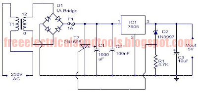
For circuits using TTL ICs the supply voltage is a great concern and a slight increase in supply from the rated 5V may damage the IC. Using fuses alone does not solve the problem because a fuse may take several milliseconds to blow off and that’s enough time for the IC to get damaged. In this circuit a crowbar scheme is used in which a triac short circuits the power supply and burns the fuse.
The burning time of the fuse is not a concern because the power supply is already shorted by the triac and the output voltage will be zero. Operation of the circuit is when the output voltage exceeds 5.6 volts the zener diode D2 conducts and switches ON the triac T1.Now T1 acts as a closed switch, shorting the circuit. The output voltage drops to zero and fuse gets burned off. The trip voltage can be varied by varying the values of D2 and R2. Since the switching of triac takes place within few micro seconds there will be no damage to the TTL ICs or any other such voltage sensitive components in the load circuit. For the transformer T1 can be a 230 V AC primary, 12v secondary, 2A step-down transformer. All capacitors must be rated at least 25V. If 1A Bridge is not available, make one using four 1N4007 diodes.

For circuits using TTL ICs the supply voltage is a great concern and a slight increase in supply from the rated 5V may damage the IC. Using fuses alone does not solve the problem because a fuse may take several milliseconds to blow off and that’s enough time for the IC to get damaged. In this circuit a crowbar scheme is used in which a triac short circuits the power supply and burns the fuse.
The burning time of the fuse is not a concern because the power supply is already shorted by the triac and the output voltage will be zero. Operation of the circuit is when the output voltage exceeds 5.6 volts the zener diode D2 conducts and switches ON the triac T1.Now T1 acts as a closed switch, shorting the circuit. The output voltage drops to zero and fuse gets burned off. The trip voltage can be varied by varying the values of D2 and R2. Since the switching of triac takes place within few micro seconds there will be no damage to the TTL ICs or any other such voltage sensitive components in the load circuit. For the transformer T1 can be a 230 V AC primary, 12v secondary, 2A step-down transformer. All capacitors must be rated at least 25V. If 1A Bridge is not available, make one using four 1N4007 diodes.
Subscribe to:
Posts (Atom)