My Geo Map

Sponsor Links

AmericasBest.com

27 July 2009

FM Transmitter Circuit Type Versatile

This is a design circuit diagram of a versatile FM transmitter. This circuit doesn’t have a coil. The circuit is simple and easy to assemble. This circuit is work based on gate logic concept. This is the figure of the circuit.


The gate N1 acts as a buffer for strengthening the signals from the condenser microphone. The inverter N2 with its associated components forms a radio frequency oscillator in the FM region. The varicaps diode BB109 is used for frequency modulating the audio signal to the carrier wave generated by the oscillator. Inverters N4 t0 N6 are used to drive the antenna. As the N4, N5, N6 are connected in parallel their effective output impedance is very less and can easily drive the antenna. All electrolytic capacitors must be rated 10V.

This circuit is use a 10 cm long wire as antenna. Gates N1 to N6 belong to same IC CD4069. The battery can be a 9V transistor radio battery. Adapters are not recommended because they would induce noise in the circuit.


Fire Alarm Circuit Based on Transistor

This is a design for circuit o f the fire alarm. This circuit is work based on 3 transistors. When there is a fire breakout in the room the temperature increases. This ultra compact and low cost fire alarm senses fire breakout based on this fact. This is the figure of the circuit.


The operation of the circuit will based on this explanation. The transistor BC177 (Q1) is used as the fire sensor here. When the temperature increases the leakage current of this transistor also increases. The circuit is designed so that when there is an increase in the leakage current of Q1, transistor Q2 will get biased. As a result when there is a fire breakout the transistor Q2 will be on. The emitter of Q2 (BC 108) is connected to the base of Q3 (AC 128).So when Q2 is ON Q3 will be also ON. The transistor Q3 drives the relay which is used to drive the load ie, light, bell, horn etc as an indication of the fire. The diode D1 is used as a free wheeling diode to protect it from back EMF generated when relay is switched. All capacitors are electrolytic and must be rated at least 10V.

The load can be connected through the C, NC, NO points of the relay according to your need. The calibration can be done using a soldering iron, and a thermo meter. Switch ON the power supply. Keep the tip of soldering iron near to the Q1.Same time also keep the thermometer close to it. When the temperature reaches your desired value adjust R1 so that relay gets ON. This is not a latching alarm, when the temperature in the vicinity of the sensor decreases below the set point the alarm stops. The circuit can be powered using a 9V battery or a 9V battery eliminator.

Door Handle Alarm Circuit Using Transistor

The automatic door handle alarm circuit gives a audible alarm and glows a LED when somebody touches the handle of the door. The circuit is latching type and continues to produce sound until it is switched off.


The transistor Q1 is wired as an astable multi vibrator whose output is used to bias transistor Q2 to conduction. As a result the transistor q3 and LED are in OFF state. When someone touches the handle, the capacitance of the human body damps the oscillations of Q1.The cuts the biasing of Q2 and it goes OFF.As a result the current flows to the base of Q3 , it conducts and LED glows. If the switch S1 is ON the transistor pairs Q4&Q4 which is wired in the latching mode is triggered and the Buzzer Z1 is activated. When the person removes his hand from door handle the LED goes OFF but the buzzer continues to beep. The only way to mute the buzzer is to open the switch S2. All capacitors must be rated 15V.

A 9V battery or 9V DC power supply can be used to power the circuit. To make L1 wind 25 turns of 0.4 mm enameled copper wire on resistor R2 and solder the ends of the wire to the resistor leads. This unit will stand for the R2 as well as L1 because both are parallel in the circuit. A readily available 10mH inductor can be used for L2. Connect the point A in the circuit to the door handle using a long wire.

Dew Sensitive Switch Circuit Using LM358

This is a simple design circuit that can be used to switch ON or OFF a device when the dew present in the surrounding atmosphere crosses a set value. This circuit uses a dew sensitive resistive element and a comparator based on LM 358 to perform the above said operation. This is the figure of the circuit.


In operation of the circuit, at normal condition the resistance of dew sensor element will be low and so the voltage drop across it. So the voltage at the non inverting pin of LM358 (IC1) will be less than the voltage at the inverting input of the LM358.So the output of the op amp will be low. This keeps the opto coupler (MCT2E) deactivated. When the dew increases the resistance of the element increases and so do the voltage across it. Now the voltage at the non inverting pin of LM358 (IC1) will be higher than the voltage at the inverting input of the LM358.So the output of the op amp will be switched to high. This in turn activates the opto coupler. The LED glows to indicate it. As a result we get an opto coupler activated and de activated according to the amount of dew in the atmosphere. The output pins of opto coupler pin (5&4) can be used to control the external device.

Diode D1, resistors R6&R3 and capacitor C1 is employed here to derive the power for the circuit directly from mains. The dew sensor is hard to find in market. But it can be easily obtained from a old VCR. Also the type no of the sensor is not so important here. Try with any thing you get. I used one from a old Hitachi VCR. LM 358 is a dual op amp. Here only one op amp inside it is used.

Computer Microphone Circuit

This circuit was submitted and design by Lazar Pancic from Yugoslavia. The sound card for a PC generally has a microphone input, speaker output and sometimes line inputs and outputs. The mic input is designed for dynamic microphones only in impedance range of 200 to 600 ohms. Lazar has adapted the sound card to use a common electret microphone using this circuit. He has made a composite amplifier using two transistors. This is the figure of the circuit.


This is the explanation about the principle work of the circuit. The BC413B operates in common emitter to give a slight boost to the mic signal. This is followed by an emitter follower stage using the BC547C. This is necessary as the mic and circuit and battery will be some distance from the sound card, the low output impedance of the circuit and screened cable ensuring a clean signal with minimum noise pickup.

Automatic Loudness Control Circuit

This is a simple design for automatic loudness control in audio. A simple approach to this problem can be done inserting a circuit in the preamplifier stage, capable of varying automatically the frequency response of the entire audio chain in respect to the position of the control knob, in order to keep ideal listening conditions under different listening levels. This is a figure of the circuit.


The circuit is shown with SW1 in the "Control-flat" position, i.e. without the Automatic Loudness Control. In this position the circuit acts as a linear preamplifier stage, with the voltage gain set by means of Trimmer R7. Switching SW1 in the opposite position the circuit becomes an Automatic Loudness Control and its frequency response varies in respect to the position of the control knob by the amount shown in the table below. C1 boosts the low frequencies and C4 boosts the higher ones. Maximum boost at low frequencies is limited by R2; R5 do the same at high frequencies.

This is a list component that must using for built the circuit.

P1 10K Linear Potentiometer (Dual-gang for stereo)

R1, R6, R8 100K 1/4W Resistors
R2 27K 1/4W Resistor
R3, R5 1K 1/4W Resistors
R4 1M 1/4W Resistor
R7 20K 1/2W Trimmer Cermet

C1 100nF/63V
C2 47nF/63V
C3 470nF/63V
C4 15nF/63V
C5, C9 1µF/63V
C6, C8 47µF/63V
C7 100pF/63V

IC1 TL072 Dual BIFET Op Amp

SW1 DPDT Switch (four poles for stereo)

AM Receiver Circuit Using Transistor

This is the simple design and sensitivity and selectivity of the receiver are good. This circuit is use a compact three transistor, regenerative receiver with fixed feedback. The circuit is based on transistor as core of the operation. The transistor that is used is BC549. This is the figure of the circuit.


The tuned circuit is designed for medium wave, but the circuit will work up to much higher frequencies if a different tuning coil and capacitor are used. Q1 and Q2 form a compound transistor pair featuring high gain and very high input impedance. This is necessary so as not to unduly load the tank circuit. Q1 operates in emitter follower, Q2 common emitter, self stabilizing bias is via the 120k resistor and the tuning coil. As Q2 operates in common emitter its base voltage will be a V be drop higher than ground or about 0.71V in my test sample. The 120k resistor provides regenerative feedback, between Q2 output and the tank circuit input and its value affects the overall performance of the whole circuit.

The tuning coil can be salvaged from an old AM receiver. However to make your own wind about 50 to 60 turns of 26 swg enamel coated copper wire over a 3/8 inch ferrite rod about 3 inches long. This circuit is powered by 9 VDC.

Active Band Pass Filters

Active band pass filters are simply filters constructed by using operational amplifiers as active devices configured to simulate inductors. Active band pass filters are used largely at audio frequencies where otherwise the size of the inductor would become prohibitive. In this figure is multiple feedback band pass (MFBP) type which uses capacitors of equal value and leads us to simplified calculations.


Finally pick a convenient value for C which if reasonably large, leads to smaller values of resistance and consequently some aid in reducing noise. Valuable feedback (no pun intended) from readers using rate-this-page (see below and on every other page) indicates the following needs clarification. The 100 uF capacitor above is purely part of the power supply reservoir and has nothing to do with the filter itself. The two 10K resistors are part of the power supply biasing of the op amps because we are not using positive and negative power supplies. The capacitor and resistor values are simply the value of C you choose to use and the resistor values result from the following calculations. It's that simple.

1 KHz Sine Wave Generator Circuit

This is a design circuit for generates a good 1 KHz sine wave adopting the inverted Wien bridge configuration (C1-R3 & C2-R4). It features a variable output, low distortion and low output impedance in order to obtain good overload capability. The figure is shown in below.


The bulb must be a low current type (12V 40-50mA or 6V 50mA) in order to obtain good long term stability and low distortion. Distortion @ 1V RMS output is 0.15% using a 12V 40mA bulb, raising to 0.5% with a 12V 100mA one. Using a bulb differing from specifications may require a change of R6 value to 220 or 150 Ohms to ensure proper circuit's oscillation. Set R5 to read 1V RMS on an Audio mili voltmeter connected to the output with R7 rotated fully clockwise, or to view a sine wave of 2.828V Peak-to-Peak amplitude on the oscilloscope. With C1, C2 = 100nF the frequency generated is 100Hz and with C1, C2 = 1nF frequency is 10 KHz but R5 requires adjustment. High gain transistors are preferred for better performance.
Component Part:
R1 5K6
R2 1K8
R3, R4 15K
R5 500R 1/2W Trimmer Cermet
R6 330R 1/4W Resistor
R7 470R Potentiometer
C1, C2 10nF/63V
C3 100µF/25V
C4 470nF/63V
Q1, Q2 BC238 25V 100mA NPN Transistors
LP1 12V 40mA Filament Lamp Bulb (See Notes)
J1 Phone chassis Socket
SW1 SPST Slider Switch
B1 9V PP3
Clip for 9V PP3 Battery

23 July 2009

Pulse Generator And Signal Tracer Circuit Using Transistor

This is a simple circuit that can used to generate narrow pulses at about 700-800Hz frequency. The pulses, containing harmonics up to the MHz region, can be injected into audio or radio-frequency stages of amplifiers, receivers and the like for testing purposes. This circuit is built by two transistor. This is the figure of the circuit.


Operation of the circuit is Q1 & Q2 form a complementary unstable multi vibrator, whose operating frequency is set mainly by R3, C2 & C3 values. Output pulses are taken at Q2 Collector and applied to the probe by means of decoupling capacitor C1. D1 provides a symmetrical shape for the output waveform. If an earclip or headphone jack is plugged into J1, the connection from Q2 Collector and C1 - C2 is broken by the switch incorporated into J1: in this case the circuit becomes a two-stage amplifier. If you intend to use the circuit to test valve operated devices C1 must be a 630V type. Working with low voltage supply transistor devices the voltage of C1 can be lowered to 63 or 100V. A crystal (high impedance) earpiece is a good solution, provided you substitute J1 with a mono switched jack socket.

In below is the listing component that can be used to built up the circuit.
R1 1M 1/4W Resistor
R2, R4 2K7 1/4W Resistors
R3 150K 1/4W Resistor
C1 2n2/630V
C2, C3 4n7/ 63V
D1 1N4148 75V 150mA Diode
Q1 BC547 45V 100mA NPN Transistor
Q2 BC557 45V 100mA PNP Transistor
SW1 SPST miniature Slider Switch (See Notes)
J1 Stereo switched 3mm. Jack socket (See Notes)
Probe Metal Probe 3 to 5 cm. long
Clip Miniature Crocodile Clip
B1 1.5V Battery (AA or AAA cell etc).

Parking Sensor Circuit Using LM324

This is a design circuit can be used for sensing the distance between the rear bumper of the car and any obstacle behind the car. The distance can be understood from the combination of the LEDs (D5 to D7) glowing. At 25cm D7 will glow, at 20 cm D7&D6 will glow and at 5cm D7, D6 and D5 will glow. When the obstacle is beyond 25 cm none of the above LEDs will glow. This circuit is based on LM324 as core the system.


Operation work of the circuit is explanation in the next. Two ICs are used in the circuit. The IC1 (NE555) is wired as an astable multivibrator for driving the IR Diode D1 to emit IR pulses. The operating frequency of the transmitter is set to be 120Hz.The IR pulses transmitted by D1 will be reflected by the obstacle and received by the D2 (IR photo diode).The received signal will be amplified by IC2a.The peak of the amplified signal will be detected by the diode D4 and capacitor C4.R5 and R6 compensates the forward voltage drop of D4.The output voltage of the peak detector will be proportional to the distance between car’s bumper and obstacle. The output of peak detector is given to the inputs of the other three comparators IC2b,IC2c and IC2d inside the IC2(LM324).The comparators switch the status LEDs according to the input voltage their inverting inputs and reference voltages at their non inverting inputs. Resistances R7 to R10 are used to set the reference voltages for the comparators.

The D1 & D2 must be mounted close (~2cm) to each other, looking in same direction. The D1 can be a general purpose IR LED. The D2 can be general purpose IR photo diode with sun filter. For proper working of the circuit, some trial and error is needed with the position of D1 and D2 on the dash board. All capacitors must be rated 25V.


Computer Microphone Circuit


This circuit was submitted and design by Lazar Pancic from Yugoslavia. The sound card for a PC generally has a microphone input, speaker output and sometimes line inputs and outputs. The mic input is designed for dynamic microphones only in impedance range of 200 to 600 ohms. Lazar has adapted the sound card to use a common electret microphone using this circuit. He has made a composite amplifier using two transistors. This is the figure of the circuit.


This is the explanation about the principle work of the circuit. The BC413B operates in common emitter to give a slight boost to the mic signal. This is followed by an emitter follower stage using the BC547C. This is necessary as the mic and circuit and battery will be some distance from the sound card, the low output impedance of the circuit and screened cable ensuring a clean signal with minimum noise pickup.

Automatic Loudness Control Circuit

This is a simple design for automatic loudness control in audio. A simple approach to this problem can be done inserting a circuit in the preamplifier stage, capable of varying automatically the frequency response of the entire audio chain in respect to the position of the control knob, in order to keep ideal listening conditions under different listening levels. This is a figure of the circuit.


The circuit is shown with SW1 in the "Control-flat" position, i.e. without the Automatic Loudness Control. In this position the circuit acts as a linear preamplifier stage, with the voltage gain set by means of Trimmer R7. Switching SW1 in the opposite position the circuit becomes an Automatic Loudness Control and its frequency response varies in respect to the position of the control knob by the amount shown in the table below. C1 boosts the low frequencies and C4 boosts the higher ones. Maximum boost at low frequencies is limited by R2; R5 do the same at high frequencies.

This is a list component that must using for built the circuit.
P1 10K Linear Potentiometer (Dual-gang for stereo)

R1, R6, R8 100K 1/4W Resistors
R2 27K 1/4W Resistor
R3, R5 1K 1/4W Resistors
R4 1M 1/4W Resistor
R7 20K 1/2W Trimmer Cermet

C1 100nF/63V
C2 47nF/63V
C3 470nF/63V
C4 15nF/63V
C5, C9 1µF/63V
C6, C8 47µF/63V
C7 100pF/63V

IC1 TL072 Dual BIFET Op Amp

SW1 DPDT Switch (four poles for stereo)

AM Receiver Circuit Using Transistor

This is the simple design and sensitivity and selectivity of the receiver are good. This circuit is use a compact three transistor, regenerative receiver with fixed feedback. The circuit is based on transistor as core of the operation. The transistor that is used is BC549. This is the figure of the circuit.


The tuned circuit is designed for medium wave, but the circuit will work up to much higher frequencies if a different tuning coil and capacitor are used. Q1 and Q2 form a compound transistor pair featuring high gain and very high input impedance. This is necessary so as not to unduly load the tank circuit. Q1 operates in emitter follower, Q2 common emitter, self stabilizing bias is via the 120k resistor and the tuning coil. As Q2 operates in common emitter its base voltage will be a V be drop higher than ground or about 0.71V in my test sample. The 120k resistor provides regenerative feedback, between Q2 output and the tank circuit input and its value affects the overall performance of the whole circuit.

The tuning coil can be salvaged from an old AM receiver. However to make your own wind about 50 to 60 turns of 26 swg enamel coated copper wire over a 3/8 inch ferrite rod about 3 inches long. This circuit is powered by 9 VDC.

1 KHz Sine Wave Generator Circuit

This is a design circuit for generates a good 1 KHz sine wave adopting the inverted Wien bridge configuration (C1-R3 & C2-R4). It features a variable output, low distortion and low output impedance in order to obtain good overload capability. The figure is shown in below.


The bulb must be a low current type (12V 40-50mA or 6V 50mA) in order to obtain good long term stability and low distortion. Distortion @ 1V RMS output is 0.15% using a 12V 40mA bulb, raising to 0.5% with a 12V 100mA one. Using a bulb differing from specifications may require a change of R6 value to 220 or 150 Ohms to ensure proper circuit's oscillation. Set R5 to read 1V RMS on an Audio mili voltmeter connected to the output with R7 rotated fully clockwise, or to view a sine wave of 2.828V Peak-to-Peak amplitude on the oscilloscope. With C1, C2 = 100nF the frequency generated is 100Hz and with C1, C2 = 1nF frequency is 10 KHz but R5 requires adjustment. High gain transistors are preferred for better performance.

Component Part:
R1 5K6
R2 1K8
R3, R4 15K
R5 500R 1/2W Trimmer Cermet
R6 330R 1/4W Resistor
R7 470R Potentiometer
C1, C2 10nF/63V
C3 100µF/25V
C4 470nF/63V
Q1, Q2 BC238 25V 100mA NPN Transistors
LP1 12V 40mA Filament Lamp Bulb (See Notes)
J1 Phone chassis Socket
SW1 SPST Slider Switch
B1 9V PP3
Clip for 9V PP3 Battery

The Transistor Tester Circuit

This is a very simple design circuit that can be used to check the hfe of transistors. Both PNP and NPN transistors can be checked using this circuit. Hfe as high as 1000 can be measured by using this circuit. The circuit is based on two constant current sources build around transistors Q1 and Q2. This is the figure of the circuit.


Operation of the circuit is the Q1 is a PNP transistor and the constant current flows in the emitter lead. The value of constant current can be given by the equation; (V D1 -0.6)/ (R2+R4).The POT R4 can be adjusted to get a constant current of 10uA.

The Q2 is an NPN transistor and the constant current flows into the collector lead. The value of this constant current can be given by the equation; (VD2-0.6)/(R3+R5).The POT R5 can be adjusted to get a constant current of 10uA.This constant current provided by the Q1 circuit if the transistor under test is an NPN transistor and by Q2 circuit if the transistor under test is a PNP transistor is fed to the base of transistor under test. This current multiplied by the hfe flows in the collector of the transistor and it will be indicated by the meter. The meter can be directly calibrated to read the hfe of the transistor. The Zener diodes must be rated at least 400mW. J1 and J2 are transistor sockets.

Sound Operated Flip Flop Circuit

This is a design circuit in which the status of the output pins of a Flip Flop IC can be toggled by using sound. This circuit is based on LM324 IC. This is the figure of the circuit.


Processing operation of the circuit is a condenser microphone is used for picking up the sound. The first two op amp is in the IC1 LM324 is used to amplify the sound picked by the condenser microphone. The third op amp inside LM324 is wired as a level detector. When ever the voltage produced due to sound have a level more than that of the reference voltage at pin 5 of the third op amp, its output (pin 7) goes high, triggering the flip flop IC1 CD 4027.

As a result the state of the output pins of CD 4027 (pin 1 & pin 2) toggles for each burst of sound. The circuit can be powered from 4, 5 V DC. The mic M1 is a condenser mic. All capacitors must be rated 10V. The sensitivity of the circuit can be adjusted by varying the preset R9.

Medium Power FM Transmitter Circuit Using Transistor

This is a design circuit diagram of a moderate power FM transmitter circuit. This circuit is built operation by two transistors. This is a figure of complete circuit.


Operation of this circuit is explain as the voice signals picked by the microphone will be amplified by the transistor Q1.The second transistor is wired as an oscillator operating in the FM band. The output of T1 is given to the base of T2.T2 performs the modulation also. The tank circuit comprising of components L1 and C6 determines the frequency of the signal, and can be varied by adjusting C6.The capacitor C7 couples the FM signal to the antenna. The inductor L1 can be made by making 6 turns of 0.8mm enameled copper wire on a 5.5mm diameter/4.5mm length plastic former.

With a matching antenna and proper tuning this transmitter can have range up to 100 meter. The Antenna A1 can be a 1M long wire. The circuit can be powered from a9V PP3 battery.

Intelligent Trailing Switch Circuit

This is a design effective circuit in which the equipments connected at the so called trailing sockets will run only if the equipment connected at the control socket is switched on. For example, let’s connect a motor is connected to the control socket and a lamp is connected at the trailing socket. The lamp will glow only when the motor is running. This is the figure of the circuit.


Explanation of the operation circuit is when the load connected at the control circuit is switched on, the load current flows through the diodes and as a result there will a voltage drop across the diodes. This voltage drop is sufficient enough to switch on the sensitive triac T1 and the equipments connected at the trailing sockets gets power supply. The components R2 and C1 forms a snubber circuit which protects the triac from transient fluctuations. The triac T1 must be a 600V, 8A, high sensitive gate type like TIC 225M. Fit the triac with a heat sink. The maximum load that can be connected at the trailing socket is 1000W. Take at most care while handling this circuit as it is connected to 230V AC.

Almost all equipments like motors, drills, blenders, fan, old TV, radio, amplifiers etc can be connected at the control socket. In case of modern TV, computers, amplifiers, etc the power switch does not completely isolate the equipment and the equipment will draw a small amount of current in the standby mode which is sufficient enough to trigger the triac. Such equipments cannot be used on the control socket because it makes the trailing equipments ON even if the control equipment is OFF.

High Impedance DC Voltmeter Circuit Using Op Amp

This is a design for a high impedance DC voltmeter. This circuit is design with built by uA741 IC. This IC is a op-amp non-inverting DC amplifier. The IC have negative feedback that is through a DC meter requiring 1mA for full scale deflection. This is the figure of the circuit.


The principle work of this circuit is since R6 is 100 Ohms, the meter will show full scale reading when the DC input voltage to pin3 is equal to the voltage drop across R6, viz 0.1 volts. Choice of R1 and R2 for getting different voltage ranges are shown in the table. The diodes D1 and D2 protect the IC from accidental excessive input voltages and diodes D3 and D4 protect the meter from overloads. The circuit can be powered from a +9V/-9V dual power supply.

The meter M1 can be a 1mA FSD DC ammeter. The values of R1 & R2 for different voltage ranges can be obtained from the table is given below.

Digital Stop Watch Using NE555 Timer IC

This is s design of digital stop watch circuit that built around timer IC LM555 and 4-digit counter IC MM74C926 with multiplexed 7-segment LED display. This is the figure of the circuit.


MM74C926 consists of a 4-digit counter, an internal output latch, NPN output sourcing drivers for common cathode, 7-segment display and an internal multiplexing circuitry with four multiplexing outputs. The counter advances on negative edge of the clock. The clock is generated by timer IC LM555. The circuit works off a 5V power supply. It can be easily assembled on a general-purpose PCB. Enclose the circuit in a metal box with provisions for four 7-segment displays, rotary switch S1, start/stop switch S2 and reset switch S3.

For operation this circuit is explanation in the next. First, reset the circuit by pressing S3 so that the display shows ‘0000.’ Now open switch S2 for the stop watch to start counting the time. If you want to stop the clock, close S2. Rotary switch S1 is used to select the different time periods at the output of the unstable multi vibrator (IC1). This circuit is powered by 5V DC. That power supply can take from regulator power supply. You can read in this site about the regulator that can be used.

Audio Clipping Indicator Circuit

This is a design circuit can be used to identify whether there is a clipping in a particular wave form. Clipping is a phenomenon in which the amplitude of a particular waveform drops before it reaches the expected limit. This circuit glows an LED as an indication if the signal under test has clipping. The circuit is very useful in sorting out distortion problems in amplifiers. This is a figure of the schematic.


The circuit is based on a window comparator based on the two op amps inside the IC1 (TL082). Operation this circuit is based on the circuit detects the positive or negative peak value reached by the input signal. The output of the op amp is combined by the two diodes D1 & D2 and drives the transistor Q1 to glow the LED.

The capacitor C5 is employed to induce a small time delay in order to detect very fast and short peaks. The POT R1 can be used to set the level of clipping at which the LED has to glow. The circuit can be used with almost all sorts of mixers, power amplifiers and preamplifiers. The circuit can be powered from a 9V PP3 battery. The POT R5 can be use to calibrate the circuit.

12V & 5V Power Supply Circuit

This is a simple approach circuit to obtain a 12V and 5V DC power supply using a single circuit. The circuit uses two ICs 7812(IC1) and 7805 (IC2) for obtaining the required voltages. This circuit is usually be make by all designer electronics and uses in microcontroller. This is the figure of the design circuit.


Operation of this circuit is the AC mains voltage will be stepped down by the transformer T1, rectified by bridge B1 and filtered by capacitor C1 to obtain a steady DC level. The transformer T1 can be a 230V primary, 15V secondary, 1A step-down transformer. The IC1 regulates this voltage to obtain a steady 12V DC. The output of the IC1 will be regulated by the IC2 to obtain a steady 5V DC at its output. In this way both 12V and 5V DC are obtained. For safety this circuit you must using a fuse. The fuse F1 can be of 1A. The switch S1 can be a SPST ON/OFF switch. The LED D1 acts as a power ON indicator. If 1A bridge B1 is not available, make one using four 1N4007 diodes.

Such a circuit is very useful in cases when we need two DC voltages for the operation of a circuit. By varying the type number of the IC1 and IC2, various combinations of output voltages can be obtained. If 7806 is used for IC2, we will get 6V instead of 5V.Same way if 7809 is used for IC1 we get 9V instead of 12V.


5V Power Supply Circuit Using Overvoltage Protection

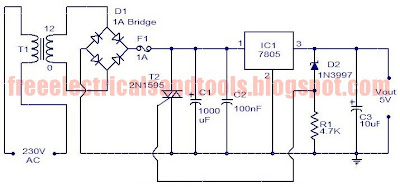
This is a design for power supply circuit. This circuit can produce source voltage 5V. This circuit is built by TTL IC’s. But this design is simple design. This is the figure of the circuit.


For circuits using TTL ICs the supply voltage is a great concern and a slight increase in supply from the rated 5V may damage the IC. Using fuses alone does not solve the problem because a fuse may take several milliseconds to blow off and that’s enough time for the IC to get damaged. In this circuit a crowbar scheme is used in which a triac short circuits the power supply and burns the fuse.

The burning time of the fuse is not a concern because the power supply is already shorted by the triac and the output voltage will be zero. Operation of the circuit is when the output voltage exceeds 5.6 volts the zener diode D2 conducts and switches ON the triac T1.Now T1 acts as a closed switch, shorting the circuit. The output voltage drops to zero and fuse gets burned off. The trip voltage can be varied by varying the values of D2 and R2. Since the switching of triac takes place within few micro seconds there will be no damage to the TTL ICs or any other such voltage sensitive components in the load circuit. For the transformer T1 can be a 230 V AC primary, 12v secondary, 2A step-down transformer. All capacitors must be rated at least 25V. If 1A Bridge is not available, make one using four 1N4007 diodes.

21 July 2009

Simple Car Battery Charger

This is a circuit for battery charger. But the circuit can places in a car. This is a simple design and useful to make it. In this circuit there is facility for monitoring the charging current and voltage. This is the figure of the car battery charger.


The circuit is based on the IC MC78T12ABT from Freescale. The IC is nothing but a 7812 in TO-3 package with 3A capacity. The transformer T1 steps the mains voltage to 15V AC and diodes D1&D2 does the job of rectification. The transformer T1 can be a 230V primary; 15-0-15V, 3A secondary step down transformer. Capacitor C1 does the filtering and C2 acts as a decoupling capacitor. The ground terminal of IC1 is lifted to 2.1V using the diodes D3, D4 and D5. So the output from the IC1 will be a regulated 14.1V (12+2.1).The battery is charged via diode D6.The D6 blocks reverse flow of current from battery to charging circuit when the mains power is not available. Meter M1 shows the charging current and M2 shows the charging voltage. Fuse F1 can be a 1A fuse. The meter M1 can be a 3A ammeter. Meter M2 can be a 20V volt meter.

Regulated Dual Power Supply Circuit Using Regulator IC

The circuit is use to regulation dual power supply that provides +12V and -12V from the AC mains. A power supply like this is a very essential tool on the work bench of an electronic hobbyist. This is the figure of the schematic of the circuit.


This circuit is built by LM7812 and LM7912 for the voltage regulator IC. The transformer T1 steps down the AC mains voltage and diodes D1, D2, D3 and D4 does the job of rectification. Capacitors C1 and C2 does the job of filtering.C3, C4, C7and C8 are decoupling capacitors. IC 7812 and 7912 are used for the purpose of voltage regulation in which the former is a positive 12V regulator and later is a negative 12V regulator. The output of 7812 will be +12V and that of 7912 will be -12V. Transformer T1 can be a 230V primary; 15-0-15 V, 1A secondary step-down transformer. Fuse F1 can be a 500mA fuse. Capacitor C1, C2, C5 and C6 must be rated at least 50V.


Electromagnetic Sensor Circuit Using 741 IC

This is a design schematic to sensor the electromagnetic field. This circuit is based or built by 741 IC. This IC is an op-amp. The circuit can detect the field even hidden wrings. This is the figure of the schematic.


A 1mH inductor is used for sensing the electric field. The electric field will induce a small voltage in the sensor inductor and this induced voltage is amplified by the op amp. The headphone connect at the output of the op amp will give an audio indication of the electric field. For example, the electric field around a main transformer can be heard as a 50 Hz hum. The POT R4 can be used to adjust the gain of the amplifier. By keeping the sensor inductor near to a telephone line, you can even hear the telephone conversations. All electrolytic capacitors must be rated at least 15V. The switch S1 can be a slide type ON/OFF switch. The POT R4 can be used to adjust the gain. It is better to have a radial type inductor for L1.

12 V – 15A Voltage Regulator Circuit

This is a circuit diagram of a powerful 12V regulator. The circuit can deliver up to 15 A of current. The circuit is based on work of the LM7812 IC as the core of the circuit. This is the figure of the circuit.


The common voltage regulator IC 7812(IC1) is used to keep the voltage at steady 12V and three TIP 2599 power transistors in parallel are wired in series pass mode to boost the output current.

The operation work of the circuit is the 7812 can provide only up to 1A and rest of the current is supplied by the series pass transistors. The 15A bridge B1 does the job of rectifying the stepped down AC input. The capacitor C1, C2 and C3 act as filters. The 1A fuse F1 protects the IC1 from over current in case if the pass transistors fail. The 15A fuse F2 protects the entire circuit (especially the pass transistors) from over current. The T1 can be a 230V AC primary, 18V secondary, 15A type transformer. The B1 can be a 15A bridge. If 15A Bridge is not available, make one using four RURG1520CC diodes. The IC1 and transistors must be mounted on heat sinks.

11 July 2009

Two transistor tone controller

This is a simple design for tone control, but in this circuit it built by two transistors. The transistor that can be used is BC109C. This is the figure of the ton control circuit.


The operation of the circuit is the transistor Q1 is wired an emitter follower to provide sufficient current gain and input impedance. The second transistor is used to voltage amplify the signal in. The network of resistance and capacitors connected between emitter of Q1 and base of Q2 is used to control the tone. Variation in the value of these components varies the audio response of the system. This circuit can provide a maximum attenuation and boost of 10decibel on 10 KHz and 60 Hz frequency ranges. The input and output must be connected with respect the ground. POT R5 can be used to control bass. POT R8 can be used to control treble.

FM Tracking Transmitter Circuit

This is a design for the tracking transmitter of audio tone in FM band frequency. The circuit can be used a signal transmitter or remote control transmitter. The circuit is use only the available components. The range of the transmitter is 100 m in the distance using 9V power supply and with a matching antenna. The circuit is built by 555 timer IC for producing the audio tone and based on JFET as core the circuit. This is figure the circuit.


The operation of the circuit is the first JFET (Q1) is wired as a Hartley oscillator which is frequency modulated by the audio tone. The second (Q2) JFET is wired as a buffer to isolate the oscillator based on Q1 from the antenna. The diode D1 is used as a varactor here. The diode is reverse biased by the ramping voltage produced at the pin 6&2 of the IC1.This results in the change of junction capacitance of reverse biased diode, which in turn alters the frequency of the oscillator to attain the frequency modulation. The inductor L1 can be made by winding 5 turns of 18 SWG enameled copper wire on a 3/8 inch long, 3/16 inch diameter plastic tube .The coil must be tapped at the center. The antenna can be a 20cm long wire.


06 July 2009

Stereo Line Driver Circuit Using Transistor

This is the schematic diagram of a low cost stereo line driver. The circuit is based only two transistors and few passive components. This is the figure of the circuit.


The description work of the circuit is each BC 109C transistor is wired as an emitter follower for driving each channel. The voltage gain of the emitter follower is unity, but it has a high current gain and low output impedance, ideal for driving long cables. The output impedance is around 16 Ohms at 1KHz.Since voltage gain is unity power amplifiers must be used at the listening end in order to drive loud speakers. The circuit can be powered from a 12V battery or 12V DC power supply. A power amplifier is needed at the listening end because the emitter follower has only unity voltage gain. The inputs and outputs must be connected with respect to ground as shown in circuit.

50 W Amplifier Circuit Using Transistor

This is a design of circuit that is very rugged and reasonably power amplifier circuit that can be used for any audio applications. The circuit is designed such that most of the components are not critical and can be easily replaced by nearest values. This is makes it ideal to assemble from your electronics junk box. This is the figure of the circuit;


The operation of the amplifier is the amplifier produces 60W rms at 50V supply on a 8 Ohm load. The capacitor C1 controls low frequencies and capacitor C2 controls high frequencies. The circuit is basically a class B amplifier. The transistors 2N 3055 serves the function of driving the speaker. The other transistor functions as pre amplifiers for the driver stage. This is the basic scheme of the circuit. The maximum power level of amplifier can be set by adjusting the 500 Ohm POT connected with the BC107 transistor.

The are some notes for this circuit. The circuit can be powered using a 50 V DC power supply with 5A current rating. It is up to 60 V can be given to the circuit. Any way the power supply must be well regulated and filters to avoid noise. The amplifier is adjusts the 500 ohm POT to obtain optimum performance. Volume control can be attained by connecting a 10 K POT in series to the input of the amplifier.

12V/15A Voltage Regulator Circuit

This is a design of the circuit diagram of a powerful 12V regulator that can deliver up to 15 A of current. This circuit is built by MOSFET and LM7812 IC. This is the figure of the circuit;


The common voltage regulator IC 7812(IC1) is used to keep the voltage at steady 12V and three TIP 2599 power transistors in parallel are wired in series pass mode to boost the output current. The 7812 can provide only up to 1A and rest of the current is supplied by the series pass transistors.

The operation of the power supply is when the 15A bridge B1 does the job of rectifying the stepped down AC input. The capacitor C1, C2 and C3 act as filters. The 1A fuse F1 protects the IC1 from over current in case if the pass transistors fail. The 15A fuse F2 protects the entire circuit (especially the pass transistors) from over current. This circuit can be assembly on a good quality PCB. The T1 can be a 230V AC primary, 18V secondary, 15A type transformer. If 15A Bridge is not available, make one using four RURG1520CC diodes. The IC1 and transistors must be mounted on heat sinks. The B1 can be a 15A bridge.

01 July 2009

Audio Amp Output Power Limiter Circuit

This is a simple peak limiter - performance is quite respectable, and it can be used with conventional amps using bipolar transistors, MOSFETs. The gain control element is a Light Dependent Resistor (LDR). These are blessed with a few very useful features for our purposes, one of which is low distortion even at quite high signal levels. Being light activated, all we need is a LED to provide illumination when the preset power level is reached. This is the figure of the circuit;


The operation of the circuit is a 10k resistor selected for the input, and although this is lower than I would like, many power amps have a relatively low input impedance and too much signal would be lost. The LDR simply shunts the signal to earth when it is illuminated. A single unit should control both channels of the power amp as shown. If only one channel is needed, then delete the components for "Right", including the associated light pipe.

The value of R3 must be selected based on the amplifier power. For a 100W amp, a value of 1.8k is about right, but it is likely that a little experimentation will be needed. As a rough guide, the table below will be helpful, and it is probable that the value from the table will be OK. The idea is to limit the current through the LED to a sensible maximum.

AM Radio Circuit Using Transistor

The circuit for a powerful AM transmitter using ceramic resonator/filter of 3.587 MHz is presented here. This circuit is based on transistor for the core operation of the circuit. Resonators/filters of other frequencies such as 5.5 MHz, 7 MHz and 10.7 MHz may also be used. Use of different frequency filters/resonators will involve corresponding variation in the value of inductor used in the tank circuit of oscillator connected at the collector of transistor T1. This is the figure of the circuit;


The AF input for modulation is inserted in series with emitter of transistor T1 (and resistor R4) using a transistor radio type audio driver transformer as shown in the circuit. Modulated RF output is developed across the tank circuit which can be tuned to resonance frequency of the filter/resonator with the help of gang condenser C7. The next two stages formed using low-noise RF transistors BF495 are, in fact, connected in parallel for amplification of modulated signal coupled from collector of transistor T1 to bases of transistors T2 and T3. The combined output from collectors of T2 and T3 is fed to antenna via 100pF capacitor C4.

The circuit can be easily assembled on a general-purpose PCB. The range of the transmitter is expected to be one to two kilometers. The circuit requires regulated 9 volt power supply for its operation. Note: Dotted lined indicates additional connection if a 3-pin filter is used in place.

300W Subwoofer Power Amplifier Circuit Using Transistor

This is a design of power amplifier for subwoofer with power 300W. This circuit is based on transistor PNP and NPN for the core of the operation. In another, the high power is required, another 4 output transistors are recommended, wired in the same way as Q9, Q10, Q11 and Q12, and using 0.33 ohm emitter resistors. For completed figure, we can see in the figure in below.


Connections are provided for the Internal SIM (published elsewhere on the Project Pages), and filtering is provided for RF protection (R1, C2). The input is via a 4.7uF bipolar cap, as this provides lots of capacitance in a small size. Because of the impedance, little or no degradation of sound will be apparent. A polyester cap may be used if you prefer - 1uF with the nominal 22k input impedance will give a -3dB frequency of 7.2Hz, which is quite low enough for any sub.

All three driver transistors (Q4, 5 & 6) must be on a heat sink, and D2 and D3 should be in good thermal contact with the driver heat sink. Neglect to do this and the result will be thermal runaway, and the amp will fail. For some reason, the last statement seems to cause some people confusion - look at the photo below, and you will see the small heat sink, 3 driver transistors, and a white "blob" (just to the left of the electrolytic capacitor), which is the two diodes pressed against the heat sink with thermal grease.

The input stage is a conventional long-tailed pair, and uses a current sink (Q1) in the emitter circuit. I elected to use a current sink here to ensure that the amp would stabilise quickly upon application (and removal) of power, to eliminate the dreaded turn on "thump". The amp is actually at reasonably stable operating conditions with as little as +/-5 volts! Note also that there are connections for the SIM (Sound Impairment Monitor), which will indicate clipping better than any conventional clipping indicator circuit. See the Project Pages for details on making a SIM circuit. If you feel that you don't need the SIM, omit R4 and R15.

Advertisement