When a Modern loudspeakers boxes condition are relatively insensitive to overdriving signals, however it is still important to limit the power driving it to avoid clipping of the audio signal. A broken sound from an overdriven loudspeaker is not only annoying to the the ears but also the loudspeaker itself can be damaged by the continous uncontrolled signal peaks. This is the figure of the schematic;
My Geo Map

Sponsor Links

Showing posts with label Sound. Show all posts
Showing posts with label Sound. Show all posts
27 June 2020
10 September 2009
Phone Recorder Circuit
This is a schematic for recording the conversation in telephone. One constructed, this switch will allows you to automatically turn on your tape recorder when you pick up the handset of your telephone. This circuit is designed to work for the newer 1.5V and 3V tape recorders as well as the usual 6V or 12V ones. This circuit is control based on transistor and FET’s. Looking in the figure of schematic.

The circuit is fall into two part and these can be easily seen in the schematic. On the left are the connections to each telephone line and to the MIC socket of the tape recorder. The diode and capacitors ensure that no DC voltages pass through to the input of the MIC while the RC network clips large transients. On the right is the circuit which detects when the handset has been lifted and which then turns on the FET. The trim pot adjusts the voltage level of this circuit. The voltage of the normal telephone line is between 40 to 60 volts (depending on country and telephone system.) When you pick up the handset of the telephone the voltage falls to between 6 and 12 volts. It is this drop in voltage which is used to control the tape recorder through the REMOTE connector. When the line voltage is high the base of the BC548 is pulled high so the transistor is turned on. This pulls the gate of the FET down to less than 1 volt. This shuts off the FET.
When the line voltage falls (that is, the handset is picked up) the BC548 will turn off, adjust the variable resistor if it does not. So the FET gate potential rises to the 10 volts set by the zener diode. This turns the FET on to high efficiency conduction mode. Different recorders may have different polarities in their REMOTE sockets. To allow for this a PCB mounted switch has to be added to the board which will reverse the polarity of the REMOTE switch just by switching it.


The circuit is fall into two part and these can be easily seen in the schematic. On the left are the connections to each telephone line and to the MIC socket of the tape recorder. The diode and capacitors ensure that no DC voltages pass through to the input of the MIC while the RC network clips large transients. On the right is the circuit which detects when the handset has been lifted and which then turns on the FET. The trim pot adjusts the voltage level of this circuit. The voltage of the normal telephone line is between 40 to 60 volts (depending on country and telephone system.) When you pick up the handset of the telephone the voltage falls to between 6 and 12 volts. It is this drop in voltage which is used to control the tape recorder through the REMOTE connector. When the line voltage is high the base of the BC548 is pulled high so the transistor is turned on. This pulls the gate of the FET down to less than 1 volt. This shuts off the FET.
When the line voltage falls (that is, the handset is picked up) the BC548 will turn off, adjust the variable resistor if it does not. So the FET gate potential rises to the 10 volts set by the zener diode. This turns the FET on to high efficiency conduction mode. Different recorders may have different polarities in their REMOTE sockets. To allow for this a PCB mounted switch has to be added to the board which will reverse the polarity of the REMOTE switch just by switching it.


Shut Off Tone Generator Circuit
This is a circuit for tone generator. This circuit is once the switch to the 9V power supply is connected, the alarm will trigger at a frequency of approximately 1.27 kHz. It will remain ON for duration of approximately 170 seconds or 2.8 minutes before it stopped. This circuit is work with based on 555 IC. This is the figure of the circuit.

In this circuit, we used two 555 timers. U2 is configured as a timer in astable mode. Once triggered, it will emit a frequency from its output at pin 3 that will drive a Q1 transistor. Q1 transistor will turn ON and OFF according to the frequency of the circuit. It will in turn used to drive a 8 ohm loud speaker to emit a loud audible sound. The frequency of the sound can be adjusted by changing the values of R3= 47K, R4= 33K and capacitor C1=10nF. Change the values of these components and by using the formula for astable mode, the frequency of the sound can be obtained.
U1 circuit is used as a delay circuit which is configured as a mono stable mode. It is a one shot multivibrator that will generate a pulse at its output at pin 3 which will disable the astable circuit U1. In this circuit, pin 2 of U1 will go to logic 0 when the power supply is connected via the capacitor E1 and hence circuit U2 is immediately triggered.

In this circuit, we used two 555 timers. U2 is configured as a timer in astable mode. Once triggered, it will emit a frequency from its output at pin 3 that will drive a Q1 transistor. Q1 transistor will turn ON and OFF according to the frequency of the circuit. It will in turn used to drive a 8 ohm loud speaker to emit a loud audible sound. The frequency of the sound can be adjusted by changing the values of R3= 47K, R4= 33K and capacitor C1=10nF. Change the values of these components and by using the formula for astable mode, the frequency of the sound can be obtained.
U1 circuit is used as a delay circuit which is configured as a mono stable mode. It is a one shot multivibrator that will generate a pulse at its output at pin 3 which will disable the astable circuit U1. In this circuit, pin 2 of U1 will go to logic 0 when the power supply is connected via the capacitor E1 and hence circuit U2 is immediately triggered.
25 August 2009
Sound Shifter Using IC HT8950
This is a design circuit for super sound shifter circuit that can be used to add effects to the input sound signal. The circuit is ideal for incorporating in toys and adds great fun. The circuit can be also used in mixers and recorders. The circuit is based on IC HT 8950 from Holtek. The IC HT8905 is a single chip CMOS sound modulator IC which produces seven steps of shift in the frequency of the given sound. This is the complete figure of the circuit.

This circuit is producing a dramatic change in the output. The IC produces two effects robotic and vibrato. The two effects can be selected using push buttons. An audio amplifier IC HT82V 733 is also included in the circuit to amplify the sound out put of HT 8950 to a reasonable level. The 50 K POT can be used as a volume control. The circuit can be powered from a 4.5 V DC supply. The desired sound effects can be selected from the push buttons. All capacitors must be rated 10V. For speaker is using 8 ohm speaker can be used as the load.

This circuit is producing a dramatic change in the output. The IC produces two effects robotic and vibrato. The two effects can be selected using push buttons. An audio amplifier IC HT82V 733 is also included in the circuit to amplify the sound out put of HT 8950 to a reasonable level. The 50 K POT can be used as a volume control. The circuit can be powered from a 4.5 V DC supply. The desired sound effects can be selected from the push buttons. All capacitors must be rated 10V. For speaker is using 8 ohm speaker can be used as the load.
20 August 2009
Intercom Circuit Using Transistor
This is a design circuit of intercom circuit. This design is simple but effective intercom circuit that is based fully on transistors. The circuit is based on a three stage RC coupled amplifier. This is the figure of the circuit.

When the pushbutton S2 is pressed, the amplifier circuit wired around T1 & T2 becomes an astable multi vibrator and starts producing the ringing signals. These ringing signals will be amplified by the transistor T3 to drive the speaker. When the push button S2 is released the circuit will behave as an ordinary amplifier and you can talk to the other side through it.
To construct a two way intercom, make two identical copies of the circuit given below and connect it according to the given connection diagram. The stand by current consumption of this circuit is around 20mA. Use 9V PP3 battery for powering the circuit. The Mic M1 can be condenser micro phone. Use a slide switch for switch S1.S1 can be used to power the circuit. Use push to ON type push button switch for S2.

When the pushbutton S2 is pressed, the amplifier circuit wired around T1 & T2 becomes an astable multi vibrator and starts producing the ringing signals. These ringing signals will be amplified by the transistor T3 to drive the speaker. When the push button S2 is released the circuit will behave as an ordinary amplifier and you can talk to the other side through it.
To construct a two way intercom, make two identical copies of the circuit given below and connect it according to the given connection diagram. The stand by current consumption of this circuit is around 20mA. Use 9V PP3 battery for powering the circuit. The Mic M1 can be condenser micro phone. Use a slide switch for switch S1.S1 can be used to power the circuit. Use push to ON type push button switch for S2.
03 August 2009
Computer Microphone Circuit
This circuit was submitted and design by Lazar Pancic from Yugoslavia. The sound card for a PC generally has a microphone input, speaker output and sometimes line inputs and outputs. The mic input is designed for dynamic microphones only in impedance range of 200 to 600 ohms. Lazar has adapted the sound card to use a common electret microphone using this circuit. He has made a composite amplifier using two transistors. This is the figure of the circuit.
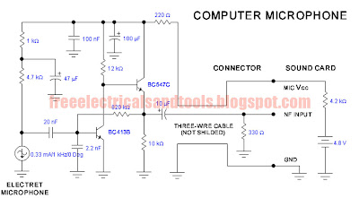
This is the explanation about the principle work of the circuit. The BC413B operates in common emitter to give a slight boost to the mic signal. This is followed by an emitter follower stage using the BC547C. This is necessary as the mic and circuit and battery will be some distance from the sound card, the low output impedance of the circuit and screened cable ensuring a clean signal with minimum noise pickup.

This is the explanation about the principle work of the circuit. The BC413B operates in common emitter to give a slight boost to the mic signal. This is followed by an emitter follower stage using the BC547C. This is necessary as the mic and circuit and battery will be some distance from the sound card, the low output impedance of the circuit and screened cable ensuring a clean signal with minimum noise pickup.
27 July 2009
Computer Microphone Circuit
This circuit was submitted and design by Lazar Pancic from Yugoslavia. The sound card for a PC generally has a microphone input, speaker output and sometimes line inputs and outputs. The mic input is designed for dynamic microphones only in impedance range of 200 to 600 ohms. Lazar has adapted the sound card to use a common electret microphone using this circuit. He has made a composite amplifier using two transistors. This is the figure of the circuit.

This is the explanation about the principle work of the circuit. The BC413B operates in common emitter to give a slight boost to the mic signal. This is followed by an emitter follower stage using the BC547C. This is necessary as the mic and circuit and battery will be some distance from the sound card, the low output impedance of the circuit and screened cable ensuring a clean signal with minimum noise pickup.

This is the explanation about the principle work of the circuit. The BC413B operates in common emitter to give a slight boost to the mic signal. This is followed by an emitter follower stage using the BC547C. This is necessary as the mic and circuit and battery will be some distance from the sound card, the low output impedance of the circuit and screened cable ensuring a clean signal with minimum noise pickup.
Subscribe to:
Posts (Atom)


