My Geo Map

Sponsor Links

AmericasBest.com

26 October 2009

Precision Relaxation Oscillator Circuit Using LM131

This is a circuit for precision oscillator that is the basic design using a voltage to frequency converter and based on op amp LM131. Basically, this IC, like any V/F converter, is a precision relaxation oscillator that generates a frequency linearly proportional to the input voltage. As might be expected, the circuit has a capacitor, CL, with a saw tooth voltage on it. This is the figure of the circuit.


The general description about this circuit is the circuit is a feedback loop that keeps this capacitor charged to a voltage very slightly higher than the input voltage, VIN. If VIN is high, CL discharges relatively quickly through RL, and the circuit generates a high frequency. If Vin is low, CL discharge slowly, and the converter puts out a low frequency. When CL discharges to a voltage equal to the input, the comparator triggers the one-shot. The one-shot closes the current switch and also turns on the output transistor. With the switch closed, current from the current source recharges CL to a voltage somewhat higher than the input. Charging continues for a period determined by RT and CT. At the end of this period, the one-shot returns to its quiescent state and CL resumes discharging. [Schematic’s source: National Semiconductor, Inc].

Stepper Motor Controller

This is one kind of design control circuit. This a motor stepper controller circuit that is a simple, low cost, and accurate position controls. Stepper motor can be driven by circuit mounted close to the motor, and controlled by a remote control circuit through long cable. The interesting thing of this circuit is that the power for both motor and the driver circuit is carried over two wires, the same wires that carry the control signal. This is the figure of the circuit.


LMC555 CMOS timer integrated circuit (IC1) generates 200 microsecond pulses to step the motor and control its speed. The speed of the motor can be changed by changing the frequency of this pulse, R1 variable resistor is provided for this purpose. At the output of IC1 (pin 3), a negative going clock pulse drive the gate of IRL530N (Q1) power FET that momentarily turns OFF and disconnects the driver board from ground. This power interruption sends a signal to the motor driver to step the motor. The rotation direction is controlled by the polarity of the voltage applied to the driver circuit through interconnect lines L1 and L2. MPSA05 Bipolar NPN transistor Q2 and MPSA55 PNP transistors Q3 and Q4 invert the pulse from pin 3, pull the drain of Q1 UP when it is OFF. Toggle switch S1 sets its direction by switching polarity. Pushbutton S2 starts and stops the motor by turning the clock on and off.

Parts
C1 – .47 MFD 35 volt tantalum
C2 – 1000 MFD 35 volt electrolytic
C3 – .1 MFD 50 volt metalized film
C4 – .001 MFD 50 volt metalized film
C5 – 100 MFD 16 volt electrolytic
R1 – 5MEG potentiometer
R2, R8, R10 – 100K 1/8 watt 5%
R3 – .56K 1/8 watt 5%
R4, R5, R7 – 10K 1/8 watt 5%
R6 – 2K 1/8 watt 5%
R9 – 4.7K 1/8 watt 5%
Q1 – MPSA05 NPN transistor
Q2, Q3 – MPSA55 PNP transistor
Q4, Q5, Q6, Q7, Q8 – IRL530N Hexfet
D1, D2, D3 – 1N914 silicon diode
D4, D5 – 1N4752 zener diode
D6 – 1N4004 rectifier
BR1 - 2 AMP 400 volt bridge rectifier
IC1 – LMC555 CMOS timer
IC2, IC5 – 78L05 5 volt regulator
IC3 – CD4013 dual D flip flop
IC4 – CD4070 quad exclusive or
S1 – momentary N/O push button switch
S2 – double pole double throw toggle switch
T1 – DC or AC adapter transformer to match motor
IC socket – 1 eight pin
IC sockets – 2 fourteen pin
Terminal blocks – 2 two position
M1, M2 – two phase unipolar 24 volts


20 October 2009

Transformer Voltage Booster Circuit: DC-DC Step-Up Switching Regulator Using Transistors

A DC-to-DC step-up converter is traditionally implemented using transformer, working by converting the DC voltage to AC Voltage, step-up it using transformer, then rectify and filter the transformer’s output to get a higher DC voltage. Using a switching method, we can step-up a voltage without a transformer. We just need an inductor which is driven by a switching transistor to boost the voltage. This is the figure of the circuit.


The most interesting this is that circuits use a discrete component: no integrated chip is required, only few transistors with few passive components. Because the switching topology is a boost converter, this circuit cannot be operated as step-down regulator, so the output will always be higher than the input. The voltage output is depend on the load because the feedback mechanism, through the zener diode, will maintain the output at about 14 volt, regardless the voltage input variation and load current variation. The current from the voltage divider will flow through the zener diode if the output goes higher than the nominal value, and this condition will stop the oscillator built around the 2N3904 transistors. Stopping the oscillator will drop the output voltage and thus maintain the required voltage level at the output. This transistor (Q1, Q2, and Q3) form a Schmidt trigger that drive the final transistor Q4 (the switching transistor 2N3053).

This circuit is suitable for battery booster, if you need to run your 12 volt equipments on your old car that is provide only a 6V supply from the battery. The output of this voltage double can be adjusted by changing the voltage divider, or for easier adjustment, you can replace the 4,7K resistor with a 5K potentiometer. Using a good inductor (low resistance), you can achieve up to 80% efficiency, and up to 2 Watt power can be delivered to the load. [Circuit's schematic diagram source: Bill Bowden's circuit collection]

Swimming Pool Solar Heat Control Circuit

This is a swimming pool solar heating panel pump control. The circuit in below is use an external thermistor that is attached to the solar panel in a manner that will allow it to sense heat generated by direct exposure to the sun. This circuit is controlled by IC TC621-C. This is the figure of the circuit.


A thermistor with a resistance of about 100 kΩ at 25°C should be selected. One such thermistor is the ACW-027 from Ketema, which can be clamped around a pipe in the solar panel. This circuit will energize the pump when the sun is heating the panels and turn off the pump when the sky is cloudy or the sun goes down. To prevent rapid cycling of the pump during partly cloudy conditions, the hysteresis is set for a relatively wide (20°F) span. Providing low thermal impedance between the thermistor assembly and the solar panel will also prevent rapid pump cycling by adding the solar panel’s thermal time constant to the hysteresis. To select the set point resistors, consult the thermistor data sheet for the thermistor’s value at the desired temperature. For example, assume that we want the pump to turn on (high set point) at 100°F and turn off (low set point) at 80°F. [Schematic diagram source: Microchip Technology, Inc].

Negative Resistance Oscillator Circuits

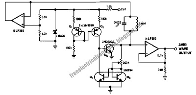
This is a circuit of negative resistance circuits. All of the preceding circuits rely on RC time constants to achieve resonance. LC combinations can also be used and offer good frequency stability, high Q and fast starting. In the circuit, signal input is control and amp using op amp LF353. This is the figure of the circuit.


In this circuit, a negative resistance configuration is used to generate the sine wave. The Q1-Q2 pair provides a 15 μA current source. Q2's collector current sets Q3's peak collector current. The 300 kΩ resistor and the Q4-Q5 LM394 matched pair accomplish a voltage-to-current conversion that decreases Q3's base current when its collector voltage rises. This negative resistance characteristic permits oscillation. The frequency of operation is determined by the LC in the Q3-Q5 collector line. The LF353 FET amplifier provides gain and buffering. Power supply dependence is eliminated by the zener diode and the LF353 unity gain follower. This circuit starts quickly and distortion is inside 1.5%.

Greatly Expanded Scale Circuit Using LM3914

This is the circuit for bar mode using LM3914 IC for great expanded scale. This circuit is only consists of some resistors circuit. This is the figure of the circuit.


Placing the LM3914 internal resistor divider in parallel with a section (230Ω) of a stable, low resistance divider greatly reduces voltage changes due to IC resistor value changes with temperature. Voltage V1 should be trimmed to 1.1V first by use of R2. Then the voltage V2 across the IC divider string can be adjusted to 200mV, using R5 without affecting V1. LED current will be approximately 10mA. [Schematic source: National Semiconductor, Inc].

Feedback Amplifier Circuit Using Transistor

This is a circuit that is design for feedback the amplifier. The circuit is used to achieve a specified amplifier gain we usually use op amp amplifier design to ease the setting of the gain. This is the figure of the circuit.


When the gain accuracy is not critical, we can use transistor feedback amplifier as the base of our amplifier design. This circuit is built by transistor. Without TR2, the circuit is taking the emitter of TR1 as the output then we can see an emitter follower circuit, the voltage variation if TR1 base cause the emitter voltage to follow the base voltage. The mechanism of the emitter follower is based on the fact that the small base-emitter current will cause a large collector- emitter current, but this current cause the emitter voltage (the voltage across the emitter resistor) to rise, and the this reaction will make the base-emitter current to decrease since the current is the result of base-emitter voltage difference.

This action and reaction is the basic of the feedback mechanism in the circuit. Now look at the TR2, this transistor amplify the collector current of the TR1, and now the feedback source is supplied from the TR2 collector through R4. TR2 make the collector current of TR1 very small, since the feedback is now handled by TR2. The current drawn by the base of TR1 becomes smaller, providing batter amplifier impedance at the input.

Driving Capacitive Load Circuit

This is a one design circuit for low impedance loads circuit using driving the capacitive loads. This circuit is combine the high output current required to slew large capacitances with appropriate frequency compensation. This circuit is based on LT1210 for control and amplified the signal input. This is the figure of the circuit.


Bridging can be used to increase the output power transferred to a transformer. Differential operation also promotes the cancellation of even-order distortion. In the figure is shown a differential application using an LT1207 as a bridge driver for HDSL. [Schematic source: Linear Technology Corporation, Inc].

Diesel and Horn Circuit for Train

This is a one module of diesel and horn train circuit. This circuit is work with built by 555 timers IC, and some op amp. This circuit is a complete system for the horn circuit. This is the figure of the circuit.


The main power supply to the system must be a regulated 12 volts DC with a minimum input from the train control AC or DC power supply of 13.5 VAC connected to pos 3 and 4 of the rectifier bridge. The ground bus of the regulated 12 volts supply must be connected to the system ground. The independent speed reference voltage is taken directly from the train speed control module or can be taken by connecting directly from the tracks to positions 5 and 6 of the rectifier bridge .The output of this bridge will always be a positive speed voltage signal whichever direction the train is going.

The 555 timer is really a poor replacement for the LM566 as a VCO (Voltage controlled oscillator) although it is linear in function a negative voltage range is needed to activate the timer and produce the RPM to relate to the actual engine speed thus the op-amp is used to invert the track positive voltage.

A Frequency Doubler Effect for Electric Guitar

This circuit is a octave shifting that is used for electric guitar is done by rectifying the original signal, just like AC to DC conversion inside your AC-DC power supply adapter. This circuit is use single supply instead of symmetric power supply. This is the figure of the circuit.


The rectifying is done by four 1N4148 silicon diodes, configured as full-wave rectifier bridges. Because the bridge is inserted inside the negative feedback of the operational amplifier (op-amp) U1B, the nonlinear characteristic of the diodes around the turn-on point (the forward bias voltage) is compensated by the op-amp’s feedback mechanism. As the result, the output of the rectifier looks like coming from ideal diode with no bias voltage needed. The pre-amp gain can be adjusting by R3 potentiometer between clean and slightly overdriven, hear the effect, and set as you want.

The R4 pot is provided to adjust the processed signal so the output level after the frequency doubling is equal to the level before entering this analog effect processor. Make R7, R8, and C3 layout as close as possible to the pin 10 of the LM324 IC (U1C) with shortest possible wiring to minimize capturing any noise. This voltage (at pin 10 U1) is the reference for internal “virtual ground” coming out from U1C output (pin 8). Make sure that the PCB tracks for this “virtual ground” (pin 8 U1) are wider than other signal tracks to give consistent reference for all op-amps. Make sure C4 and C5 have the shortest possible connection to the power pins (pin 4, pin 11) and the “virtual ground” line (pin 8).

18 October 2009

Wien Bridge Oscillator Circuit

This is a circuit that is known as wien bridge oscillator circuit. The circuit has positive and negative feedback loop. This circuit is work with control by op amp. This is the figure of the circuit.


The circuit oscillates at a frequency determined by the RC time constant at frequency and produces a sinusoidal waveform at the output voltage Vout. In many cases this circuit is used as sine wave generator which is using rail to rail op amp. [Schematic’s diagram source: Advanced Linear Devices, Inc]

Phase Shift Oscillator Circuit Using LM386

This is a design circuit of a simple inexpensive amplitude stabilized phase shift sine wave oscillator which requires one IC package, three transistors and runs off a single supply. This circuit is combination with the RC network comprises a phase shift configuration and oscillates at about 12 kHz. The remaining circuitry provides amplitude stability. Here’s the schematic figure of the circuit.


The high impedance output at Q2's collector is fed to the input of the LM386 via the 10 μF-1M series network. This circuit is using op amp LM386 causes it has fixed gain of 20. The 1M resistor in combination with the internal 50 kΩ unit in the LM386 divides Q2's output by 20. The positive peaks at the amplifier output are rectified and stored in the 5 μF capacitor. This potential is fed to the base of Q3. Q3's collector current will vary with the difference between its base and emitter voltages. Since the emitter voltage is fixed by the LM313 1.2V reference, Q3 performs a comparison function and its collector current modulates Q1's base voltage. Q1, an emitter follower, provides servo controlled drive to the Q2 oscillator.

Lead Acid Battery Charger Circuit

This is battery charger circuit that is use a fly back converter topology, and implements a current-limited power supply to charge lead-acid batteries. This circuit is control by MAX471 IC. This is the figure of the circuit.


The flyback transformer provide isolation and voltage input range flexibility, event at supply voltage lower that the battery voltage. Monitoring the charging current is done by sensing the output using MAX471 current sense amplifier. The result of the output current monitoring is then used to give a feedback to a threshold detector, to detect if the value falls below the predetermined threshold. This detection is used to switch the charger into trickle mode, when a lower voltage is applied for lower charging current. [Schematic source: Maxim Integrated Products Application Notes]

High Voltage AC Calibrator Circuit Using Op Amp

This a application circuit for calibration. This circuit is called high voltage AC calibrator circuit. In another dimension in sine wave oscillator design is stable control of amplitude. This is the figure of the circuit.


In this circuit, not only is the amplitude stabilized by servo control but voltage gain is included within the servo loop. A transformer is used to provide voltage gain within a tightly controlled servo loop. A voltage gain of 100 is achieved by driving the secondary of the transformer and taking the output from the primary. A current sensitive negative absolute value amplifier composed of two amplifiers of an LF347 quad generates a negative rectified feedback signal. This is compared to the LM329 DC reference at the third LF347 which amplifies the difference at a gain of 100. The 10 μF feedback capacitor is used to set the frequency response of the loop.

The output of this amplifier controls the amplitude of the LM3900 oscillator thereby closing the loop. As shown the circuit oscillates at 1 kHz with under 0.1% distortion for a 100 Vrms (285 Vp-p) output. If the summing resistors from the LM329 are replaced with a potentiometer the loop is stable for output settings ranging from 3 Vrms to 190 Vrms (542 Vp-p!) with no change in frequency. If the DAC1280 D/A converter shown in dashed lines replace the LM329 reference, the AC output voltage can be controlled by the digital code input with 3 digit calibrated accuracy. [Schematic diagram source: National Semiconductor, Inc]

Free Running Oscillator Circuit

This is a circuit for oscillator using astable mode operation. The basic oscillatior is using 555 timer IC. This circuit is also give mode free running oscillator. This is the figure of the circuit.


Operation of the circuit is begin, when initialy by capacitor C charged towards 2/3 V+ with Ra and Rb. When voltage on C reaches that threshold level, the discharge output in pin 7 is turning on to discharging C. Using CMOS 555 timer IC is a very wide frequency at very low of voltage spikes and dissipation can be achieved. Selections of values the Ra and Rb is limited by input leakage specification at time in pin 7, 2, and 6.

Baxandall Tone Control Circuits Using Two Transistor

This is design circuit of tone control circuit that is use very popular Baxandall configuration, a simple circuit configuration that provides boost and cut control in continuous manner. This circuit is very cheap to build, and it’s commonly implemented in commercial product. This circuit is built by two transistors. This is the figure of the schematic.


The transistors can be substituted by any general audio transistors with small current gain more than 100 (BC547, 2N3904, and many more). The supply voltage for this circuit is 9-15V DC. The components that is used is low cost and can buy in component electronics store.

15 October 2009

Wideband Output Amplifier Circuit

This is a simple design for wideband output amplifier. The wideband amplifier is suitable for use as a 50Ω transmission line driver. This circuit is built by CA3140. This is the figure of the circuit.


This circuit, when used in conjunction with the function generator and sine wave shaper circuits shown in Figures 10 and 12 provides 18VP-P output open circuited, or 9VP-P output when terminated in 50Ω. The slew rate required of this amplifier is 28V/μs (18VP-P x π x 0.5MHz).
[Schematic diagram source: Intersil Corporation].

Set or Reset Flip Flop Circuit

The circuit in below is an example of a set/reset flip flop using discrete components. This circuit is built by some components which is low cost and there is in electronic store. This is the figure of the circuit.


When power is applied, only one of the transistors will conduct causing the other to remain off. The conducting transistor can be turned off by grounding it is base through the push button which causes the collector voltage to rise and turn on the opposite transistor.

Octaver Fuzz Guitar Effect Circuit

This is a design for guitar effect. This circuit is used for produces fuzz sound, so it is called fuzz effect. This circuit is built by low noise dual op amp IC and transistor. This is the figure of the circuit.


The GEU is good sounding octave fuzz, with an optional mode of just fuzz. The fuzz is a fully rectified signal and is quite chewy. For some the Fuzz alone might not be loud enough, this can be fixed by raising the value of the 820 ohm resistor and lowering the 39k one. Or one could just replace both with a normal volume pot for a more standard approach. The "struzz" is the fuzz with an octave higher signal mixed in. Good for signal notes and leads.

Maestro Fuzz Guitar Effect Circuit

This is one of kind guitar effect. This circuit is used for produces loud noise for you guitar sound. This is the figure of the circuit.


The Maestro Fuzz is reputed to be the fuzz used in the recording of the Stones’ "Satisfaction". The transistors are house numbered "991-002298" and the diode is house numbered "919-004799". They are probably all germanium devices. The use of a squelch device is somewhat unique, possibly put there to tame hiss and noise during quiet passages between notes. The two 50K pots which have their wipers connected by resistors are wired so that as one increases, the other decreases, giving a pan from one point in the circuit to another, probably changing the amount of distortion. The last 50K pot is an output level control.

Intercom Preamp Circuit Using Transistor

There are thousands of pre-amplifier circuits. These are three which have interested me and are a little different. This is a simple design circuit of intercom pre-amplifier. This circuit is built by transistor and several low cost components. Tr1 is operated in grounded base mode with input to its emitter to give low impedance input. The values shown give correct operation from 9v. This is the figure of the circuit.


High quality microphones also tend to be low impedance, typically around 600 ohms. This is low input impedance, high quality pre-amplifier of the sort that could be used in a stage mixing desk. The circuit uses a dual rail power supply - convenient because there were many op-amps in the machine. Note that Tr1 is a PNP transistor. Theoretically PNP transistors can have lower noise level than NPNs. Tr2 amplifies Tr1's output. Tr3 is simply a constant current collector load for Tr2, with its current controlled by the 180R emitter resistor. This can be altered to give more current to feed lower impedance output loads.

High Current MOSFET Toggle Switch Circuit

This is a circuit design for high current toggle switch. This circuit was adapted from the "Toggle Switch Debounced Pushbutton" by John Lundgren. It is useful where the load needs to be switched on from one location and switched off from another. Any number of momentary (N/O) switches or push buttons can be connected in parallel. This circuit is work with based on transistor as controller the circuit. This is the figure of the circuit.


The combination (10K, 10uF and diode) on the left side of the schematic insures the circuit powers up with the load turned off and the NPN transistor conducting. These components can be omitted if the initial power-on condition is not an issue. When a switch is closed, the 1uF cap voltage is connected to the junction of the 220 ohm and 33K resistors causing the circuit to change state. When the switch is opened, the cap charges or discharge to the new level through the 1M resistor, and the circuit is ready to toggle again in about 1 second. It takes a little time for the cap to move to the new level, either +V or ground. The (0.1uF) capacitor at the transistor base was added to press noise that might cause false triggering if the switches are located far away from the circuit. The circuit was tested using a 12 volt, 25 watt automotive lamp, and IRFZ44. Other MOSFETs can probably be used. [Schematic diagram source: Bill Bawden]

Dual Channel Digital Volume Control Circuit

This is a design for digital volume control. This circuit could be used for replacing your manual volume control in a stereo amplifier. This circuit is built from 7555, 74193 and dual 4066 IC. This circuit is a dual channel volume control. This is the figure of the circuit.


IC1 timer 555 is configured as an un-stable flip-flop to provide low-frequency pulses to up/down clock input pins of pre-stable up/down counter 74LS193 (IC2) via push-to-on switches S1 and S2. To vary the pulse width of pulses from IC1, one may replace timing resistor R1 with a variable resistor. Operation of switch S1 (up) causes the binary output to increment while operation of S2 (down) causes the binary output to decrement. The active high outputs A, B, C and D of the counter are used for controlling two quad bi-polar analogue switches in each of the two CD4066 ICs (IC3 and IC4). Each of the output bits, when high, short a part of the resistor network comprising series resistors R6 through R9 for one channel and R10 through R13 for the other channel, and thereby control the output of the audio signals being fed to the inputs of stereo amplifier.

Bi Stable Flip Flop Circuit

This circuit is almost same with the circuit before. But, in this circuit there are two samples for the same circuit. It is two examples of bi stable flip flops which can be toggled between states with a single push button. This is the figure of the circuit.


When the button is pressed, the capacitor connected to the base of the conducting transistor will charge to a slightly higher voltage. When the button is released, the same capacitor will discharge back to the previous voltage causing the transistor to turn off. The rising voltage at the collector of the transistor that is turning off causes the opposite transistor to turn on and the circuit remains in a stable state until the next time the button is pressed and released. Note that in the LED circuit, the base current from the conducting transistor flows through the LED that should be off, causing it to illuminate dimly. The base current is around 1 mA and adding a 1K resistor in parallel with the LED will reduce the voltage to about 1 volt which should be low enough to ensure the LED turns completely off.

Automatic Solar Power Supply Circuit

This circuit is almost same with 5V regulated solar power supply circuit. The different with circuit before is using diode 1N4148 and resistor that is parallel with solar panel. This is the figure of the circuit.


The oscillator will turn off when the output from the solar panel is above 1.3v and although the circuit does not shut down to zero current, it consumes about 3 mA, while the shut-off circuit takes about 1mA. On a bright day, the solar panel delivers 20mA to the battery, so the overall net charging current is about 15mA max. This means any data logging circuit or transmitter connected to the supply will only work at night.

To go over the purpose of the automatic section again: The automatic components turn off the 5v section so the battery can charge and store enough energy to operate a transmitter during the night hours, when it will be needed.

Audio Graphic Equalizer Circuit Using Op Amp

This is a design circuit for audio graphic equalizers, that are very common as commercial products but circuits for them are very rarely published. This circuit is a simple design circuit. The circuit is need an op-amp for amplifying the input signal. This is the figure of the circuit.


Only one gyrator stage is shown: all 7 gyrators are the same circuit, only the capacitors change, as shown in the chart. I have shown three of the seven faders to show where they go. A gyrator is a circuit using active devices and transistors to simulate an inductor. In this case the gyrator is the transistor acting with R1, R3 and C2. It could just as easily be a unity gain op-amp. The circuit includes three formulae: one which gives f, the the centre frequency of the band. The second shows how the Q is related to the capacitor ratio. The third shows the impedance presented by the circuit. Note that this includes 3 terms, the first purely resistive, the second is the capacitive contribution from C1 and the third is an inductive term from the gyrator.

5V Regulated Solar Power Supply Circuit

This is a circuit of power supply that is produces a 5 VDC voltage. This circuit is rechargeable battery using solar panel. The solar panel charges the battery when sunlight is bright enough to produce a voltage above 1.9v. A diode is required between the panel and the battery as it leaks about 1mA from the battery when it is not illuminated. This is the figure of the circuit.


How is the power supply work? The regulator transistor is designed to limit the output voltage to 5v. This voltage will be maintained over the capability of the circuit, which is about 10mA. The oscillator transistor must be a high-current type as is turned on for a very short period of time to saturate the core of the transformer. This energy is then released as a high-voltage pulse. These pulses are then passed to the electrolytic and appear as a 5v supply with a capability of about 10mA. If the current is increased to 15mA, the voltage drops to about 4V. The circuit operates at approx 50 KHz and the pulses quickly charge the electrolytic.

The 15k resistor has a 3k3 "trimmer" resistor to enable you to adjust the output to exactly 5v or slightly above 5v. Microcontrollers will work up to 5.5v but some will freeze at 5.6v, so be careful. The output voltage is monitored at the join of the 15k resistor (and 3k3) and the 2k2 resistor. The voltage at this point is exactly 0.63v (630mV) and at this voltage the regulator transistor turns ON and robs the oscillator transistor with "turn-on" voltage.

13 October 2009

Audio Graphic Equalizer Circuit Using Op Amp

This is a design circuit for audio graphic equalizers, that are very common as commercial products but circuits for them are very rarely published. This circuit is a simple design circuit. The circuit is need an op-amp for amplifying the input signal. This is the figure of the circuit.


Only one gyrator stage is shown: all 7 gyrators are the same circuit, only the capacitors change, as shown in the chart. I have shown three of the seven faders to show where they go. A gyrator is a circuit using active devices and transistors to simulate an inductor. In this case the gyrator is the transistor acting with R1, R3 and C2. It could just as easily be a unity gain op-amp. The circuit includes three formulae: one which gives f, the the centre frequency of the band. The second shows how the Q is related to the capacitor ratio. The third shows the impedance presented by the circuit. Note that this includes 3 terms, the first purely resistive, the second is the capacitive contribution from C1 and the third is an inductive term from the gyrator.

Accelerometer Amplifier Circuit

This is a circuit for accelerometer amplifier. This is a simple circuit. Precision accelerometer needs inverting mode amplifier since they are usually charge-output devices. This amplifier is convert charges into voltage output. The circuit below is an example of accelerometer with DC servo. This circuit built by IC LT1113.


The charge from the transducer is converted to a voltage by C1, which should equal the transducer capacitance plus the input capacitance of the op amp. The low frequency bandwidth of the amplifier will depend on the value of R1 • C1 (or R1 (1 + R2/R3) for a Tee network). The noise gain will be 1 + C1/CT. The time constant of the servo (1/R5C5) should be larger than the time constant of the amplifier (1/R1C1).
[Schematic source: Linear Technology Application Notes]

AM-FM Antenna Booster Circuit

This is design for antenna booster circuit. This circuit can be used to amplify the weak signal received by the antenna. This circuit is a simplest form of circuit. Antenna for AM/FM is usually not tuned for the optimal dimension of 1/4 wavelength, since we prefer small portable size. This is the figure of the circuit.


Use around 470uH coil for L1 if you use for AM frequency (700 KHz - 1.5 MHz) and use around 20uH for SW or FM receiver. For short wave performance, using this antenna booster, you’ll get a strong signal as we get from a 20-30 feet antenna, with only a standard 18″ telescopic antenna and this booster circuit. The power supply should be bypassed by a 47nF capacitor to ground, at a point that should be chosen as close as possible to L1.

Intercom Preamp Circuit Using Transistor

There are thousands of pre-amplifier circuits. These are three which have interested me and are a little different. This is a simple design circuit of intercom pre-amplifier. This circuit is built by transistor and several low cost components. Tr1 is operated in grounded base mode with input to its emitter to give low impedance input. The values shown give correct operation from 9v. This is the figure of the circuit.


High quality microphones also tend to be low impedance, typically around 600 ohms. This is low input impedance, high quality pre-amplifier of the sort that could be used in a stage mixing desk. The circuit uses a dual rail power supply - convenient because there were many op-amps in the machine. Note that Tr1 is a PNP transistor. Theoretically PNP transistors can have lower noise level than NPNs. Tr2 amplifies Tr1's output. Tr3 is simply a constant current collector load for Tr2, with its current controlled by the 180R emitter resistor. This can be altered to give more current to feed lower impedance output loads.

11 October 2009

Video Limiter Circuit

This circuit is use to avoid exceeding luminance reference level standard or to avoid exceeding the input range of digitizer (ADC), video signal is often needed to be limited. The simple way to do this is by hard limiting the signal in the positive direction (white peak clipping), but this method completely destroy all information contained in the clipped region. This circuit is based on LT1228 IC’s. This is the figure of the circuit.


The better way to limit the signal is while preserving all information contained in the signal is by soft limiting the signal, where the signal will be compressed at the above threshold region. The LT1228 is used here in a slightly unusual, closed-loop configuration. The gain of the closed-loop is set by the feedback and gain resistors (RF and RG) and the open-loop gain by the trans-conductance of the first stage times the gain of the CFA. The level at which the limiting action begins is adjusted by varying the set -current into pin 5 of the trans-conductance amplifier.
[Schematic diagram source: Linear Technology Application Notes]

Transformer Voltage Booster Circuit: DC-DC Step-Up Switching Regulator Using Transistors

A DC-to-DC step-up converter is traditionally implemented using transformer, working by converting the DC voltage to AC Voltage, step-up it using transformer, then rectify and filter the transformer’s output to get a higher DC voltage. Using a switching method, we can step-up a voltage without a transformer. We just need an inductor which is driven by a switching transistor to boost the voltage. This is the figure of the circuit.


The most interesting this is that circuits use a discrete component: no integrated chip is required, only few transistors with few passive components. Because the switching topology is a boost converter, this circuit cannot be operated as step-down regulator, so the output will always be higher than the input. The voltage output is depend on the load because the feedback mechanism, through the zener diode, will maintain the output at about 14 volt, regardless the voltage input variation and load current variation. The current from the voltage divider will flow through the zener diode if the output goes higher than the nominal value, and this condition will stop the oscillator built around the 2N3904 transistors. Stopping the oscillator will drop the output voltage and thus maintain the required voltage level at the output. This transistor (Q1, Q2, and Q3) form a Schmidt trigger that drive the final transistor Q4 (the switching transistor 2N3053).

This circuit is suitable for battery booster, if you need to run your 12 volt equipments on your old car that is provide only a 6V supply from the battery. The output of this voltage double can be adjusted by changing the voltage divider, or for easier adjustment, you can replace the 4,7K resistor with a 5K potentiometer. Using a good inductor (low resistance), you can achieve up to 80% efficiency, and up to 2 Watt power can be delivered to the load. [Circuit's schematic diagram source: Bill Bowden's circuit collection]

Touch Switch Circuit

This is a touch circuit that is used as a latching circuit to switch a LED ON and OFF by physically touching the ON metal plate or OFF metal plate. This circuit is based on logic gate for control the operation. This is the figure of the circuit.


It is important to ensure that 9V battery is used as its DC source. If one uses the mains supply to step down the voltage using a transformer for rectification and filtering to get the 9V DC supply, ensure that the transformer is designed in such a way that it follows the safety standard requirement of UL. This is important to ensure the safety of the user that is using the metal contacts to ON/OFF the LED.[Schematic diagram source: Electronics Project Design].

Phase Control Circuit

This is a simple design schematic circuit for phase control circuit. The circuit can be used to control the power delivered to an AC load. The phase control circuit can control the AC waveform, cutting the cycle to give full cycle, half cycle, zero cycle, or somewhere in between. You can say this circuit is similar to a dimmer circuit, but the switching is synchronized with the zero crossing of the waveform. This circuit is works using based on IC U208B. This is the figure of the circuit.


The benefit of switching the power in zero crossing condition is that the triacs doesn’t suffer power dissipation, thus increasing the overall efficiency. This phase control circuit is suitable for brushed AC motor, heater filament, or incandescent lamps. The IC U208B is designed as a phase control circuit in bipolar technology with internal supply-voltage monitoring. As the voltage is built up, uncontrolled output pulses are avoided by internal monitoring. Furthermore, it has internal-current and voltage synchronization. It is recommended as a low cost open-loop control. [Schematic diagram source: TEMIC TELEFUNKEN Microelectronic Application Notes]

Butterworth Second Order High Pass Filter Circuit

This is a circuit for high pass filter. This circuit is similar to low-pass filter circuit, but the position for resistors and capacitor are interchanged. This circuit is based on op-amp for the operation. LM833 IC is the op-amp that is used in the circuit. This is the figure of the circuit.


Similar with low pass design guide, the resistor and capacitor should be chosen according to the formula, and the resistor value should be:
· Much higher than equivalent leakage resistance of the capacitor.
· Much higher than the operational-amplifier’s (op-amp’s) input impedance.
· Doesn’t draw excessive current-violating the maximum allowed op-amp’s output current.

In general, for higher capacitor value, it is leakage current would be higher and you must use lower resistors to compensate the capacitor’s current leakage. [Schematic source: National Semiconductor's LM833 Application Notes]

09 October 2009

SPI Interface Circuit for Big 7 Segment LED

This circuit is uses for the general purpose Big LED with SPI serial interfacing. The circuit is using a serial-in-parallel out shift register, 74HC595 for receiving serial data from microcontroller board. This is the figure of the circuit.


For wiring the schematic is SER is for data input, SRCLK is shift clock and RCLK is Latch clock. Each data bit is shifted into the register on rising edge of the shift clock. When all data bits are shifted into the 8-bit register, the rising edge of RCLK will clock the data to be latched at each output bit, i.e. QA - QH. The Big LED is made from cheap dot LED. Each segment has five dot LED connected in series with a limiting resistor tied to +12V. The logic high at the input of ULN2003 makes the output active low, thus sinks the LED current into the chip. The driver has 7-bit for segment a, b, c, d, e, f, and g. Q1 is for optional point display.

Multiple digits can easily be made by connecting the QH to the next digit serial input bit, see the circuit below. Please note that, the shift clock and latch signal are tied to every 74HC595.


High And Low Voltage Cut Off Circuit

This is a design for protection voltage. This circuit is called as high and low voltage cut off. The circuit is using time delay for cut off the voltage. This is a low cost and reliable circuit for protecting such equipments from damages. This is the figure of the circuit.


Whenever the power line is switched on it gets connected to the appliance only after a delay of a fixed time. If there is hi/low fluctuations beyond sets limits the appliance get disconnected. The system tries to connect the power back after the specific time delay, the delay being counted from the time of disconnection. If the power down time (time for which the voltage is beyond limits) is less than the delay time, the power resumes after the delay: If it is equal or more, then the power resumes directly. This circuit is using op-amp 741 and 555 IC for control the operation.

The complete circuit is consisting of various stages. They are: - Dual rail power supply, Reference voltage source, Voltage comparators for hi/low cut offs, Time delay stage and Relay driver stage. Under normal operating conditions i.e. when the input voltage is between maximum and minimum limit the output from the both the comparators are low. The transistor Q1 is OFF and the relay is in de-energized (pole connected to N/C pin) state and the output is obtained. When the input voltage is below or above the limits set by the pre-sets R8 or R9, the output of the Op-Amps goes either low or high and diodes D1 or D2 would be forward biased depending on the situation. Transistor Q1 switches ON and the flow of current from collector to emitter energizes the relay and the output is cutoff.

3 Transistor Audio Amplifier Circuit for 80 mW

This circuit is for amplifier 80 mW uses positive feedback to get a little more amplitude to the speaker. This is a simple design for a small amplifier. This has a disadvantage in that as the output moves positive, the drop across the 470 ohm resistor decreases which reduces the base current to the top NPN transistor. Thus the output cannot move all the way to the + supply because there wouldn't be any voltage across the 470 resistor and no base current to the NPN transistor. This is the figure of the circuit.


In this circuit, the 1K load resistor is tied to the speaker so that as the output moves negative, the voltage on the 1K resistor is reduced, which aids in turning off the top NPN transistor. When the output moves positive, the charge on the 470uF capacitor aids in turning on the top NPN transistor. The original circuit in the radio used a 300 ohm resistor where the 2 diodes are shown but I changed the resistor to 2 diodes so the amp would operate on lower voltages with less distortion. The transistors shown 2n3053 and 2n2905 are just parts I used for the other circuit above and could be smaller types. Most any small transistors can be used, but they should be capable of 100mA or more current. A 2N3904 or 2N3906 are probably a little small, but would work at low volume.

The 2 diodes generate a fairly constant bias voltage as the battery drains and reduces crossover distortion. But you should take care to insure the idle current is around 10 to 20 milliamps with no signal and the output transistors do not get hot under load. The circuit should work with a regular 8 ohm speaker, but the output power may be somewhat less. To optimize the operation, select a resistor where the 100K is shown to set the output voltage at 1/2 the supply voltage (4.5 volts). This resistor might be anything from 50K to 700K depending on the gain of the transistor used where the 3904 is shown.

Advertisement